
He Li, Shanghong Zhao, Jixiang Wu, Tao Lin, Kun Zhang, Guodong Wang, Wei Jiang, Xuan Li. Generation of Reconfigurable Frequency-Conversion Signals with Full-Range Phase Shift Based on Microwave Photonics[J]. Acta Optica Sinica, 2020, 40(8): 0825001
- Acta Optica Sinica
- Vol. 40, Issue 8, 0825001 (2020)
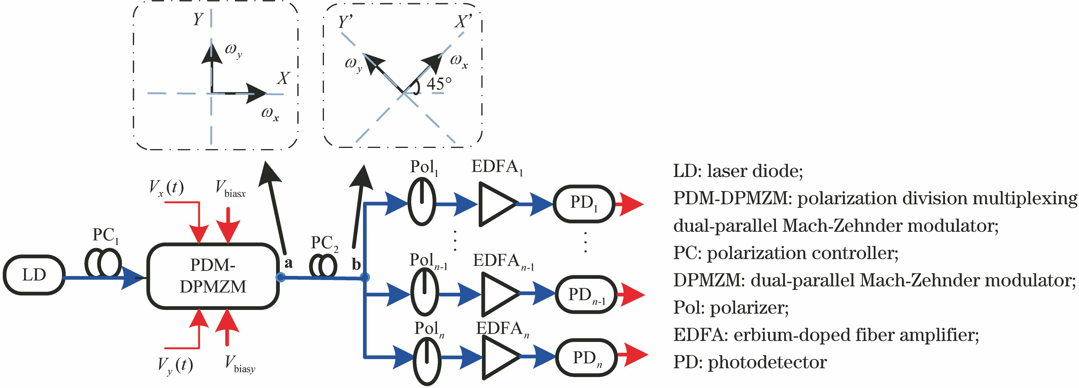
Fig. 1. Schematic diagram of the proposed frequency-doubled signal generation and frequency up-conversion or frequency down-conversion signal generation with full range phase shift
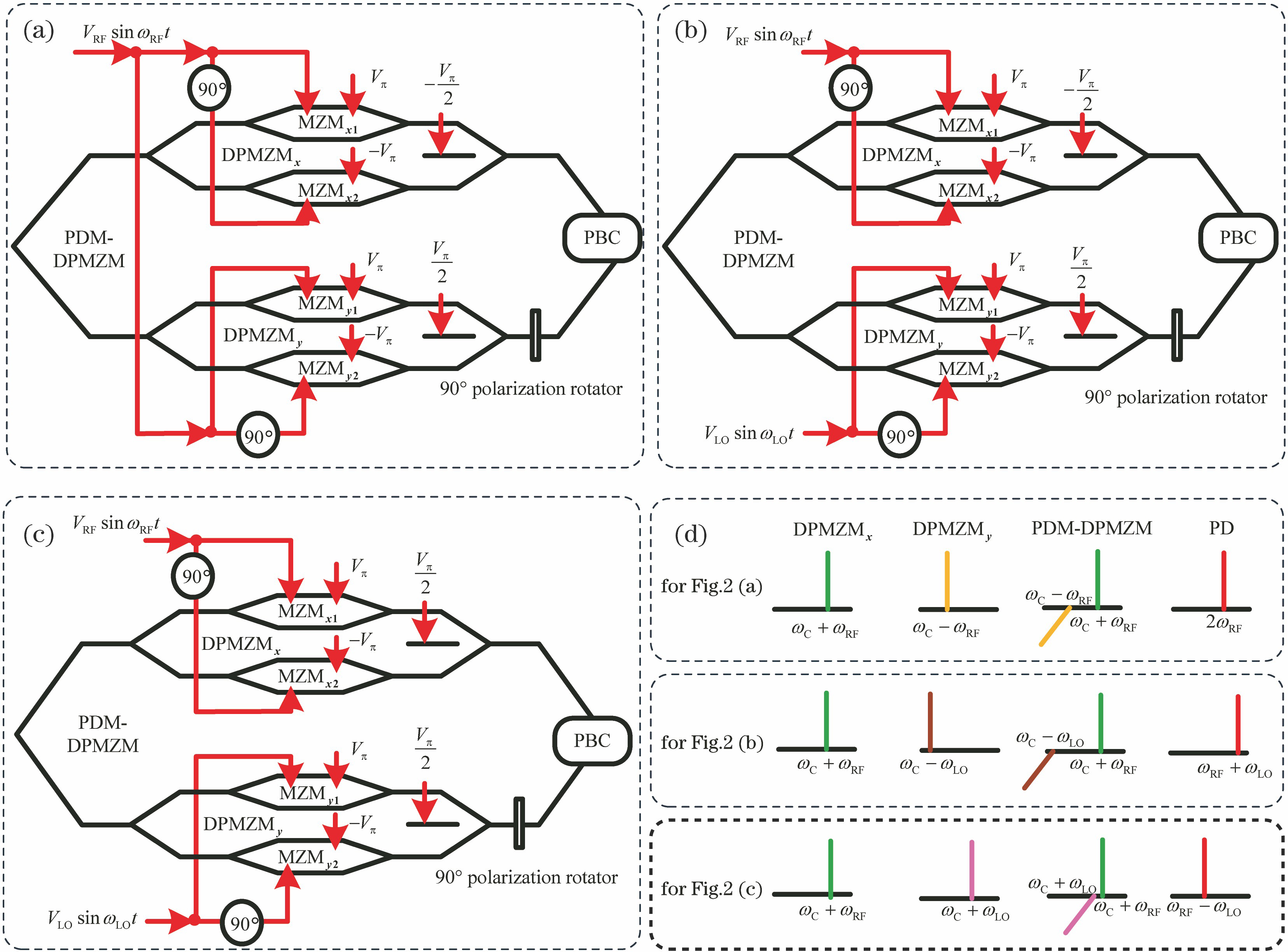
Fig. 2. RF input and DC biases of PDM-DPMZM under different phase-shift functions, and corresponding output spectrum diagram. (a) Frequency-doubled signal with phase shift; (b) frequency up-converted signal with phase shift; (c) frequency down-converted signal with phase shift; (d) output spectra for different components
Fig. 3. Schematic diagram of the proposed multiband frequency-conversion signal generation with full range phase shift in multichannel
Fig. 4. RF input and DC biases during the generation of the multiband frequency-conversion signal with phase shift in multichannel, and combination of optical sidebands. (a) RF input and DC biases; (b) combination 1; (c) combination 2
Fig. 5. Optical spectra (left) at the output of PDM-DPMZM and electric spectra (right) at the output of PD in four cases. (a) In the case of the frequency doubling operation; (b) in the case of the frequency up-conversion operation; (c) in the case of the frequency down-conversion operation; (d) in the case of the multiband frequency conversion in multichannel
Fig. 6. Waveforms of phase tuned signals in the case of the frequency doubling operation, frequency up-conversion and down-conversion operation and waveforms of phase tuned signals in different channels of multiband frequency conversion. (a) Waveforms of phase tuned frequency doubled signal (10 GHz); (b) waveforms of phase tuned frequency up-converted signal (13 GHz); (c) waveforms of phase tuned frequency down-converted signal (1 GHz); (d) waveforms of phase tuned signals in channel 1 of multiband freq
Fig. 7. Power variation of phase tuned signals under different conditions of frequency doubling, frequency up-conversion, frequency down-conversion and multiband frequency conversion. (a) Power variation under different conditions of frequency doubling, frequency up-conversion and frequency down-conversion; (b) power variation under generation of multiband frequency conversion signals
Fig. 8. Effect of DC points drift on system performance during the generation of frequency up-converted signal (13 GHz). (a) Power variation with the DC points drift; (b) USSR variation with the DC points drift
Fig. 9. Effect of DC points drift on system performance during the generation of the multiband frequency conversion signals (one of the signals with frequency of 7 GHz). (a) Power variation with the DC points drift; (b) USSR variation with the DC points drift
Fig. 10. System performance during the generation of frequency up-converted signal. (a) Power variation when Vbiasx1 and Vbiasx2 drift at the same time; (b) USSR variation when Vbiasx1 and Vbiasx2 drift at the same time; (c) power variation when Vbiasx1 and Vbia
Fig. 11. System performance when three or more DC biases drift at the same time during the generation of frequency up-converted signal. (a) Power variation; (b) USSR variation
Fig. 12. Effect of extinction ratio on USSR and the flatness of OFC. (a) USSR of frequency up-converted signal (13 GHz); (b) flatness of OFC in generation of multiband frequency conversion signals
Fig. 13. RF power and USSR of the up-converted phase tunable signal versus different polarization angles and different phase differences. (a) Polarization angle θ; (b) phase difference Δ
|
Table 1. Value of RF input and DC biases under different conditions, namely generation of frequency-doubled signal with phase shift, generation of frequency up-converted signal with phase shift and generation
|
Table 2. Parameters of PDM-DPMZM when it generates two orthogonally polarized OFCs
|
Table 3. Comparison of structure with different schemes

Set citation alerts for the article
Please enter your email address
© Copyright 2018-2021 | Chinese Laser Press. All Rights Reserved 沪ICP备15018463号-20