• Infrared and Laser Engineering
  • Vol. 51, Issue 5, 20210637 (2022)
Xingfan Chen1、2、3, Bin Li1、2、3, Xueming Li1、*, and Libin Tang2、3、*
Author Affiliations
  • 1Key Laboratory of Advanced Technique & Preparation for Renewable Energy Materials, Ministry of Education, School of Energy and Environmental Sciences, Yunnan Normal University, Kunming 650500, China
  • 2Kunming Institute of Physics, Kunming 650223, China
  • 3Yunnan Key Laboratory of Advanced Photoelectric Materials & Devices, Kunming 650223, China
  • show less
    DOI: 10.3788/IRLA20210637 Cite this Article
    Xingfan Chen, Bin Li, Xueming Li, Libin Tang. Research advances in optoelectronic devices of quantum dot-polymer nanocomposites[J]. Infrared and Laser Engineering, 2022, 51(5): 20210637 Copy Citation Text show less
    Preparation methods of quantum dots: (a) Molecular beam epitaxy; (b) Electrochemical method[12]; (c) Magnetron sputtering[32]; (d) Chemical vapor deposition[33]; (e) Hot injection method[34]; (f) Liquid phase ultrasonic method[12]
    Fig. 1. Preparation methods of quantum dots: (a) Molecular beam epitaxy; (b) Electrochemical method[12]; (c) Magnetron sputtering[32]; (d) Chemical vapor deposition[33]; (e) Hot injection method[34]; (f) Liquid phase ultrasonic method[12]
    Schematic diagram of composite preparation methods: (a) Microemulsion method; (b) In-situ polymerization method; (c) Sol-gel method; (d) Blending method
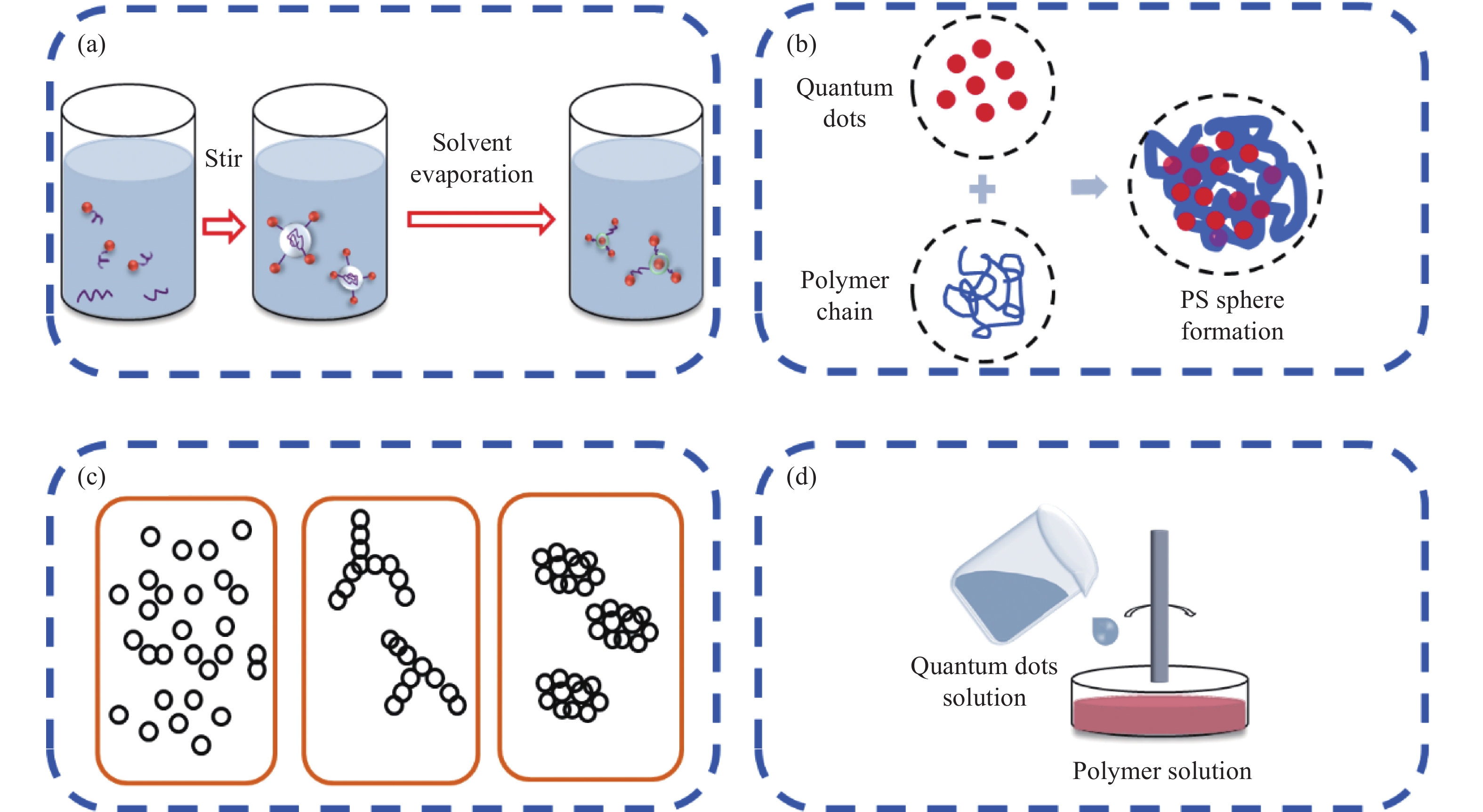
    Fig. 2. Schematic diagram of composite preparation methods: (a) Microemulsion method; (b) In-situ polymerization method; (c) Sol-gel method; (d) Blending method
    Device development process based on quantum dot-polymer nanocomposites
    Fig. 3. Device development process based on quantum dot-polymer nanocomposites
    (a) Schematic of fabricating CQDs microlaser based on the inkjet printing technique[84]; (b) QD-WLED structure diagram[85]; (c) ZnO light-emitting diode device structure diagram[86]; (d) Device structure with a combined backlight unit using a blue LED chip[87]; (e) Structure diagram of QLED device prepared by QD/ PTPA-B-CAA[88]; (f) CPB@SHFW composites structural diagram, upper right illustration is LED[89]; (g) Structure diagram of white LED prepared by hybrid microspheres of CSPbBr3-P QDs and mesoporous polystyrene (MPMs) coated with SiO2, the inset is a digital photo of the device taken at 10 mA[26]; (h) Energy band structure diagram of QLED hybrid emitting layer prepared by QD/ PTPA-B-CAA[88]; (i) Variation of PLQY of CPB@SHFW composite powder with time in water (illustration: material soaked in water for 31 days)[89]
    Fig. 4. (a) Schematic of fabricating CQDs microlaser based on the inkjet printing technique[84]; (b) QD-WLED structure diagram[85]; (c) ZnO light-emitting diode device structure diagram[86]; (d) Device structure with a combined backlight unit using a blue LED chip[87]; (e) Structure diagram of QLED device prepared by QD/ PTPA-B-CAA[88]; (f) CPB@SHFW composites structural diagram, upper right illustration is LED[89]; (g) Structure diagram of white LED prepared by hybrid microspheres of CSPbBr3-P QDs and mesoporous polystyrene (MPMs) coated with SiO2, the inset is a digital photo of the device taken at 10 mA[26]; (h) Energy band structure diagram of QLED hybrid emitting layer prepared by QD/ PTPA-B-CAA[88]; (i) Variation of PLQY of CPB@SHFW composite powder with time in water (illustration: material soaked in water for 31 days)[89]
    Photoelectric detector: (a) Device of Au/CNDS/n-Si ultraviolet photoelectric detector[93]; (b) N-GQDs photodetector schematic diagram[93]; (c) Typical Si-QD/Graphene /Si photodetector[93]; (d) Si NWs array /CuO heterostructure photodetector[93]; (e) Device structure of the PMDTC ligand[94]; (f) Schematic diagram of ZnO/P3 HT:PVK photodetector structure, the BCP layer is a composite layer of Quantum dots and polymer[95]; (g) CdTe and P3 HT photodetector structure[96]; (h) J-V curve of the device under light irradiation. Higher photocurrent density was observed under reverse bias[94]; (i) Description of 1 the generation, 2 splitting, 3 hole transport, and electron capture processes of electron-hole pairs in quantum dot polymer composites[95]
    Fig. 5. Photoelectric detector: (a) Device of Au/CNDS/n-Si ultraviolet photoelectric detector[93]; (b) N-GQDs photodetector schematic diagram[93]; (c) Typical Si-QD/Graphene /Si photodetector[93]; (d) Si NWs array /CuO heterostructure photodetector[93]; (e) Device structure of the PMDTC ligand[94]; (f) Schematic diagram of ZnO/P3 HT:PVK photodetector structure, the BCP layer is a composite layer of Quantum dots and polymer[95]; (g) CdTe and P3 HT photodetector structure[96]; (h) J-V curve of the device under light irradiation. Higher photocurrent density was observed under reverse bias[94]; (i) Description of 1 the generation, 2 splitting, 3 hole transport, and electron capture processes of electron-hole pairs in quantum dot polymer composites[95]
    MaterialsWavelength/nmSize/nmPeak/nmPhotoluminescence quantum yieldRef.
    CdS/3.550550%[18]
    CsPbI3/11-16673-692100%[19]
    ZrS2240-3603379-45453.3%[20]
    MA3Bi2Br92543.05360-54012%[21]
    MA3Bi2Cl92542-436015%[21]
    CoTe2300-4003.1400-44862.6%[13]
    Sb2Te3300-6002.3400-450/[2]
    ReS2320-4402.7420-49075.6%[22]
    N-Ti3C23603.444718.7%[23]
    ZnSeTe422-5005.346075%[24]
    CdTe4802.3-2.7/80%[25]
    CsPbBr348010/93%[26]
    WO3−WS26000.8-2.163011.6%[27]
    CdSe600-6504/97%[28]
    PbS7856-10700-1 60026%[29]
    Si8254/90%[30]
    PbTe8705-16700-1 00042%[31]
    InP/ZnS1 2002.1-4.1480-59068%[5]
    Table 1. Common quantum dot materials
    MaterialsPreparation methodWavelength/nmSize/nmPeak/nmQuantum dot content/wt%Photoluminescence quantum yieldRef.
    CdTe/PMMAThermal evaporation/2.21-3.42538-5846.113.5%[40]
    Si/PMMADoctor blading/1007500-3.335%[41]
    PbSe/PVASolution casting200-8002.111105/[42]
    SnO2/ PCz(Polycarbazole) In-situ chemical polymerization320-55015-20410-4225-20/[43]
    N-CQD/MIPs(Molecularly Imprinted Polymer)Sol-gel3303.2-4.9431//[44]
    MAPbBr3/PMMA In-situ polymerization3504543/88%[45]
    GQD/PVASolution casting350-650500/10/[46]
    CdSe/PSColloidal synthesis360-370400-500510-570//[47]
    CDs/b-PEI(Branched Polyethylenimine)one-step hydrothermal36530-50508-528/90.49%[48]
    CdTe/WPU(Waterborne Polyurethane)Casting and Evaporating3732.5-4.1528-6650.318%[49]
    TiO2/Acrylate UV polymerization3931505300.1/[50]
    InP@GaP/ZnS/PDMSSAM Encapsulating400-700/52710/[51]
    PbSe/PDTPBT(Poly(2,6-(N-(1-octylnonyl)dithieno[3,2-b:20,30-d]pyrrole)-alt-4,7-(2,1,3-benzothiadiazole)))Ligand exchange400-900150700-8000.9/[52]
    Sb2S3/PMMA One-pot synthesis450/645920%[35]
    CsPbBr3/PS In-situ photoactivated polymerization450-650/5300.244%[39]
    MAPbBr3 /PDMS Template4885.6-9.85283010%[53]
    ZnS/MQ(5-(2-methacryloylethyloxymethyl)- 8-quinolinol) In-situ polymerization4953500/40%[54]
    WS2/PVA Liquid phase exfoliation53260-120617//[55]
    C/PSSolvatothermal80012-35410-5800.422%[56]
    CeF3/PS Solution casting97527-57153010/[57]
    Table 2. Commonly used quantum dot-polymer nanocomposites
    Xingfan Chen, Bin Li, Xueming Li, Libin Tang. Research advances in optoelectronic devices of quantum dot-polymer nanocomposites[J]. Infrared and Laser Engineering, 2022, 51(5): 20210637
    Download Citation