Xinfa Zhu, Weishuai Duan, Xiancheng Meng, Xiyu Jia, Yonghui Zhang, Pengyu Zhou, Mengjun Wang, Hongxing Zheng, Chao Fan. Visible-to-near-infrared photodetectors based on SnS/SnSe2 and SnSe/SnSe2 p−n heterostructures with a fast response speed and high normalized detectivity[J]. Journal of Semiconductors, 2024, 45(3): 032703
Copy Citation Text
【AIGC One Sentence Reading】:SnSe2-based photodetectors, enhanced by SnS or SnSe heterostructures, show improved responsivity, detectivity, and response speed, paving the way for better optoelectronic devices.
【AIGC Short Abstract】:In this study, we enhanced the performance of tin diselenide-based photodetectors by creating p-n heterostructures with SnS and SnSe. These novel devices exhibit improved response speed and normalized detectivity, broadening their photoresponse range. Our approach surpasses individual 2D materials, showcasing a promising strategy for advancing SnSe2-based photodetector technology towards future commercial applications.
Note: This section is automatically generated by AI . The website and platform operators shall not be liable for any commercial or legal consequences arising from your use of AI generated content on this website. Please be aware of this.
Abstract
The emergent two-dimensional (2D) material, tin diselenide (SnSe2), has garnered significant consideration for its potential in image capturing systems, optical communication, and optoelectronic memory. Nevertheless, SnSe2-based photodetection faces obstacles, including slow response speed and low normalized detectivity. In this work, photodetectors based on SnS/SnSe2 and SnSe/SnSe2 p?n heterostructures have been implemented through a polydimethylsiloxane (PDMS)?assisted transfer method. These photodetectors demonstrate broad-spectrum photoresponse within the 405 to 850 nm wavelength range. The photodetector based on the SnS/SnSe2 heterostructure exhibits a significant responsivity of 4.99 × 10³ A?W?1, normalized detectivity of 5.80 × 1012 cm?Hz1/2?W?1, and fast response time of 3.13 ms, respectively, owing to the built-in electric field. Meanwhile, the highest values of responsivity, normalized detectivity, and response time for the photodetector based on the SnSe/SnSe2 heterostructure are 5.91 × 10³ A?W?1, 7.03 × 1012 cm?Hz1/2?W?1, and 4.74 ms, respectively. And their photodetection performances transcend those of photodetectors based on individual SnSe2, SnS, SnSe, and other commonly used 2D materials. Our work has demonstrated an effective strategy to improve the performance of SnSe2-based photodetectors and paves the way for their future commercialization.
Since 2004, significant attention has been directed towards two-dimensional (2D) materials such as graphene (GP), black phosphorus (BP), and molybdenum disulfide (MoS2), due to their extraordinary atomic-scale thickness, remarkable mechanical strength, and robust light−matter interaction[1−3]. As a nascent member of 2D materials, tin diselenide (SnSe2) is an instinct n-type Ⅳ−Ⅵ semiconductor with a Se−Sn−Se sandwich-layered structure and a bandgap of ~1 eV[4]. Furthermore, with its exceptional qualities of high carrier mobility (462 cm2/(V∙ s))[5], absorption coefficient (7.25 × 105 cm−1)[6], environmental friendliness[7], and chemical stability[8], SnSe2 is a superior material for high-sensitivity and low-consumption photodetectors, which can be widely used in image acquisition[9], information communication[10], and photo-electronic memory[11]. For example, Chen et al. fabricated a SnSe2-based photodetector via low-temperature molecular beam epitaxy, which demonstrated a normalized detectivity of 6.09 × 109 cm∙Hz1/2∙W−1 under 532 nm illumination[12]. Zhai et al. fabricated a SnSe2-based photodetector using chemical vapor deposition, which exhibited a normalized detectivity of 1.01 × 1010 cm∙Hz1/2∙W−1 and a response time of 14.5 ms under 530 nm illumination[13].
However, SnSe2-based photodetectors suffer from drawbacks such as large dark current, slow response time, and low normalized detectivity, which limits their potential for commercial application. To surmount these challenges and enhance the photodetection performance of SnSe2-based photodetectors, stacking van der Waals heterostructures has been established as an effective strategy. This is due to the unique properties of van der Waals heterostructures, including the absence of dangling surfaces, strong interlayer coupling, and ultrafast charge transfer[14, 15]. For example, Zhou et al. successfully achieved a photodetector based on a SnSe2/MoS2 heterostructure. The photodetector exhibited a normalized detectivity of 9.3 × 1010 cm∙Hz1/2∙W−1 under 500 nm illumination, which was one order of magnitude higher than that of the photodetector based on the individual SnSe2 and MoS2 components[16]. Zheng et al. reported a photodetector based on an In2Se3/SnSe2 heterostructure that outperformed the device based on the individual components by one order of magnitude, achieving a high normalized detectivity of 8.8 × 1011 cm∙Hz1/2∙W−1 under 477 nm illumination[17]. However, more efforts should be devoted to elucidating the underlying mechanisms of SnSe2-based heterostructures.
As members of the Ⅳ−Ⅵ compounds, tin mono-sulfide (SnS) and tin mono-selenide (SnSe) exhibit inherent p−type semiconductivity with an orthorhombic Sn−S (Se) layered structure[18, 19]. Given their common metallic atoms, it is both feasible and convenient to realize p−n heterostructures of SnS/SnSe2 and SnSe/SnSe2. In this work, photodetectors based on SnS/SnSe2 and SnSe/SnSe2 p−n heterostructures (denoted as the SnS/SnSe2 and SnSe/SnSe2 photodetectors) were constructed by a polydimethylsiloxane (PDMS)-assisted dry-transfer method, and then investigated. Our results demonstrate that these photodetectors manifested superior photodetection performance, encompassing enhanced responsivity, normalized detectivity, and response speed in comparison to photodetectors based on individual SnSe2, SnS, and SnSe components. This work expands the research scope of SnSe2-based photodetectors and holds great promise for future optoelectronic applications.
Experimental
Growth and characterization of materials
Single crystals of SnSe2, SnS, and SnSe were prepared by a chemical vapor transport (CVT) technique. The purity of precursors (Se, S, and Sn powders) was 99.99%, and they were purchased from Aladdin (Shanghai, CN). For SnSe2, Sn and Se powders were hermetically vacuum-sealed in a quartz tube under a vacuum of 10−5 Torr with a stoichiometric ratio of 1∶2. The precursors were heated by gradient heating: initially, the temperature was heated to 610 ℃, and held for 24 h. In the next step, the temperature was decreased to 600 ℃ and held for 120 h. Finally, they were cooled to room temperature. As to SnS, Sn and S powders were also vacuum-sealed in a quartz tube under a vacuum of 10−5 Torr with a stoichiometric ratio of 1∶1. The precursors were subjected to gradient heating: initially, the temperature was raised to 950 ℃ and held for 24 h. In the subsequent step, the temperature was lowered to 850 ℃ and held for 120 h. Finally, they were cooled to room temperature. For SnSe, Sn and Se powders were hermetically sealed with a stoichiometric ratio of 1∶1. The precursors were subjected to gradient heating: initially, the temperature was raised to 900 ℃ and maintained for 24 h. In the subsequent step, the temperature was cooled to 800 ℃ and held for 120 h. Finally, the precursors were cooled down to room temperature.
The composition and phase of the crystals were probed using an X−ray diffractometer (XRD, Smartlab, Rigaku) with Cu Kα radiation of λ = 0.15406 nm. The elemental composition and valence of the samples were assessed using an X−ray photoelectron spectroscope with an excitation source of 532 nm (XPS, Escalab 250 Xi, Thermo Fisher). The Raman spectrometer (InVia, Renishaw) was utilized to characterize the vibrational mode and material identification under the excitation source of 532 nm. The surface morphology was evaluated using an atomic force microscope (AFM, Ntegra Spectra, NT−MDT) in tapping mode and an optical microscope (OM, Olympus BX51M).
Preparation and measurement of devices
Photodetectors based on SnS/SnSe2 and SnSe/SnSe2 heterostructures were stacked by a polydimethylsiloxane (PDMS)-assisted dry-transfer method, and Au electrodes were fabricated on substrates via means of lithography and electron beam evaporation. In the case of SnS/SnSe2, SnSe2 and SnS thin films were exfoliated from their single crystals and transferred onto the substrate using PDMS films. Subsequently, SnSe2 thin films were stacked onto the SnS thin films with the assistance of an optical microscope. For SnSe/SnSe2, SnSe2 and SnSe thin films were exfoliated from their single crystals, and SnSe thin films were transferred onto the substrate using PDMS films. Subsequently, SnSe2 thin films were stacked onto the SnSe thin films with the assistance of an optical microscope. The heterostructures were then transferred onto the substrate.
The photodetection performance of the photodetectors was assessed by a self-assembled photoelectric measurement system, which comprised a probe station (PW−600, Advanced), a semiconductor device analyzer (B1500A, Keysight), a waveform generator (33500B, Keysight), and four semiconductor lasers (with a wavelength of 405, 532, 650, and 850 nm and a spot diameter of 200 μm). The power density of the lasers was ascertained by a handheld laser power and energy meter (Nova Ⅱ, Ophir).
Results and discussion
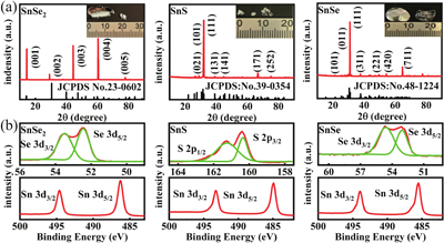
Crystals of SnSe2, SnS, and SnSe were synthesized via CVT, and their phase structures were probed by XRD. Fig. 1(a) shows XRD patterns of the as-grown crystals. The diffraction peaks are consistent with the standard cards of hexagonal-SnSe2 (JCPDS No.23-0602), orthorhombic-SnS (JCPDS No.39-0354), and orthorhombic-SnSe (JCPDS No.48-1224)[20−22]. No phases related to other impurities like SnO and SnO2 were detected. The strongest peaks corresponding to the (001), (003), (004), and (005) planes of SnSe2 indicate the c-axis preferred orientation. The (111) plane preferred orientation of SnS and SnSe, on the other hand, is indicated by the strongest peaks at 31.97° and 30.89°, respectively. The inset of Fig. 1(a) shows the corresponding optical microscopy images and all the crystals showed gray-black metallic lusters with a lateral size of >4 mm.
Figure 1.(Color online) (a) XRD patterns of the SnSe2, SnS, and SnSe crystals. The insets are the corresponding optical microscopy images. (b) XPS spectra of the SnS, SnS, and SnSe crystals.
In order to verify their chemical compositions and chemical states, XPS measurements were conducted. Fig. 1(b) illustrates the XPS spectra of the SnSe2, SnS, and SnSe crystals. For SnSe2, four peaks located at 52.5, 53.5, 485.3, and 494.6 eV are ascribed to the Se3d5/2, Se3d3/2, Sn3d5/2, and Sn3d3/2 orbitals of SnSe2, indicating the presence of the Se2− and Sn4+ states[23]. The atomic ratio of Sn to Se was determined to be 1 : 2.03 (SnSe2.03). For SnS and SnSe, two peaks located at 493.3 and 484.91 eV are attributed to the Sn3d5/2 and Sn3d3/2 orbitals of the Sn2+ state. Four peaks located at 161.3, 160.4, 54.7, and 53.1 eV correspond to the S2p1/2, S2p3/2, Se3d5/2, and Se3d3/2 orbitals of SnS and SnSe, respectively[24, 25]. The atomic ratios of Sn to S and Sn to Se were determined to be 1 : 1.08 (SnS1.08) and 1 : 1.02 (SnSe1.02), respectively.
Following the fabrication of the SnS/SnSe2 and SnSe/SnSe2 photodetectors through a polydimethylsiloxane (PDMS)−assisted dry−transfer technique, the two types of heterostructures were characterized in−situ (Fig. S1 (a)). The surface morphologies of the heterostructures were detected by AFM. As illustrated in Fig. 2(a), the SnS/SnSe2 and SnSe/SnSe2 heterostructures possess clean surfaces devoid of any impurities, undulations, or bubbles. The height profiles of the SnS/SnSe2 heterostructure reveal that the individual SnS and SnSe2 thin layers are 8 nm (~15 layers) and 9 nm (~12 layers) in thickness, respectively[4, 18]. Meanwhile, the thicknesses of the SnSe and SnSe2 in the SnSe/SnSe2 heterostructure were determined to be 9 nm (~15 layers) and 8 nm (~12 layers), respectively[19].
Figure 2.(Color online) (a) AFM results of the SnS/SnSe2 and SnSe/SnSe2 heterostructures. The insets are the corresponding height profile. (b) Raman spectra of the SnS/SnSe2 and SnSe/SnSe2 heterostructures.
Fig. 2(b) presents the Raman spectra of the SnS/SnSe2 and SnSe/SnSe2 heterostructures. And the Raman spectrum of each heterostructure can be regarded as the combination of the individual Raman spectra of SnS, SnSe, and SnSe2, thereby confirming the successful formation of the heterostructures. In the Raman spectrum of the SnS/SnSe2 heterostructure, five peaks were observed (position A1). Two of these peaks located at 109.7 and 184.6 cm−1 were attributed to the Eg and A1g vibration modes of SnSe2 (position C1), while the remaining three peaks at 161.2, 188.4, and 216.1 cm−1 were attributed to the B3g and Ag vibration modes of SnS (position B1)[26, 27]. Similarly, peaks corresponding to the Eg and A1g vibration modes of SnSe2 (position C2), as well as the , Bg, and vibration modes of SnSe (position B2) can be found in the Raman spectrum of the SnSe/SnSe2 heterostructure (position A2)[19].
The electrical characteristics of the SnS/SnSe2 and SnSe/SnSe2 photodetectors were probed by employing Au layers (50 nm) as the source and drain electrodes, while a heavily p−doped Si layer was utilized as the back gate. The output characteristics of the photodetectors were acquired by sweeping the source−drain voltage from −5 to 5 V and varying the gate−source voltage Vgs from −50 to 50 V, as illuminated in Figs. 3(a) and 3(b). The p−n junction demonstrated remarkable gate-tunable rectification behaviors, with rectification ratios of 55 and 110 observed at Vgs = 25 V for the SnS/SnSe2 and SnSe/SnSe2 photodetectors, respectively[28]. Figs. 3(c) and 3(d) depict the transfer curves of the photodetectors, which exhibited bipolar behavior attributed to the p-type SnS (SnSe) and n-type SnSe2. Notably, for the SnS/SnSe2 photodetector, the charge transport was dominated by holes when Vgs < −42.55 V, whereas electrons governed the charge transport when Vgs > −42.55 V. The mobility can be calculated using the following formula[13]:
Figure 3.(Color online) (a) and (b) Output characteristics of the SnS/SnSe2 and SnSe/SnSe2 photodetectors. The insets: the schematic diagrams and the optical images of the photodetectors. (c) and (d) Transfer characteristics on linear (left) and semi-logarithmic (right) scales of the SnS/SnSe2 and SnSe/SnSe2 photodetectors.
where and W represent the length and width of the channel (L: 5 μm and W: 4 μm), Cox is the capacitance of SiO2 with a value of 11.5 nF cm−2. The electron mobility (μe) and hole mobility (μh) of the SnS/SnSe2 photodetector were determined to be 45.3 and 41.2 cm2/(V·s), respectively, while the μh and μe values of the SnSe/SnSe2 photodetector were determined to be 21.5 and 18.3 cm2/(V·s), respectively. These values were found to be considerably higher than those of the individual SnSe2 (10 cm2/(V·s)), SnS (5.29 cm2/(V·s)), and SnSe (6.84 cm2/(V·s)) thin layers as shown in Fig. S2.
To evaluate the photodetection performance of the SnS/SnSe2 and SnSe/SnSe2 photodetectors under 405 nm illumination, the semi-logarithmic current−voltage (Ids−Vds) curves were measured at various power densities (17.8, 35.7, 75.3 μW·mm−2), as depicted in Figs. 4(a) and 4(b). The rectification behavior remained consistent as the light power density increased, with a noticeable increase in the forward current. The dark current (Idark) of both heterostructure photodetectors (0.5 μA) was observed to be one order of magnitude lower than that of SnSe2-based photodetectors (5.1 μA, Fig. S3).
Figure 4.(Color online) (a) and (b) The semi-logarithmic current−voltage curves of the SnS/SnSe2 and SnSe/SnSe2 photodetectors. (c) and (d) Transient photoresponse of the SnS/SnSe2 and SnSe/SnSe2 photodetectors. (e) and (f) Response time and photocurrent−power density plots of the two types of photodetectors.
The current−time (Ids−T) curves of the SnS/SnSe2 and SnSe/SnSe2 photodetectors were obtained at Vds = 5 V and Vgs = 0 V with a modulation frequency of 50 mHz, as presented in Figs. 4(c) and 4(d), respectively. An immediate response to the 405 nm light was observed, with the current increasing to saturation as soon as the laser was activated, and swiftly decaying to the initial state when the laser was turned off. After storage for three weeks, the photodetectors still exhibited stable and repeatable switching cycles, which can be attributed to the films possessing inert properties[29].
The response time, including the rise time (τr) and fall time (τf), was defined as the time of the photocurrent Iph (Iph= Ids − Idark) increased from 10% to 90% and decayed from 90% to 10%, respectively[30]. The rise/fall time of the SnS/SnSe2 and SnSe/SnSe2 photodetectors was estimated to be 3.13/4.54 ms and 4.74/5.18 ms, respectively, which is one order of magnitude less than that of the photodetector based on the SnSe2 thin layers (Fig. S3), as shown in Fig. 4(e). The scatter plots of photocurrent−light power intensity are displayed in Fig. 4(f), and can be fitted using the formula[16]:
where a is a constant, P is the light power intensity, and α is the fitted parameter, reflecting the efficiency of photocurrent conversion. The α values were estimated to be 0.69 and 0.60 for the SnS/SnSe2 and SnSe/SnSe2 photodetector, respectively, which are larger than that of the photodetector based on the SnSe2 thin layers (0.32, Fig. S4), indicating an increased photocurrent conversion efficiency. The observed α values were all less than 1, a behavior that has been widely reported in photodetectors based on 2D materials, owing to the presence of trap centers within the channel material[16].
Both the SnS/SnSe2 and SnSe/SnSe2 photodetectors exhibit broad-spectrum photodetection characteristics, as illustrated in Figs. 5(a) and 5(b), as well as in Fig. S5 and S6, upon illumination with wavelengths ranging from 405 to 850 nm. While the photocurrents of the two photodetectors vary under different wavelengths of illumination, their exceptional broad-spectrum photodetection abilities are evident across the near-ultraviolet to near-infrared spectrum. The photoresponsivity (R) and external quantum efficiency (EQE), two fundamental parameters for assessing a photodetector, can be derived using the following formulas[31, 32]:
Figure 5.(Color online) (a) Photocurrent−power density plots of the SnS/SnSe2 and SnSe/SnSe2 photodetectors under different wavelengths. (b) Transient photoresponse under different wavelengths. (c) Responsivity and normalized detectivity as a function of wavelength. (d) Comparison of normalized detectivity and response time of our devices with photodetectors based on other heterostructures under different wavelengths.
where λ is the incident wavelength, S is the effective area, and the size of the channel is smaller than the laser spot, therefore the effective area is 20 μm2 (length × width: 4 × 5 μm2)[33]. Typically, noise in photodetectors comprises flicker noise, thermal noise, and shot noise[34]. The noise current (IN) of the SnS/SnSe2 and SnSe/SnSe2 photodetectors can be derived from the fast Fourier transform of the dark current (see Fig. S7)[35]. At frequencies lower than 14.7 Hz (12.5 Hz), flicker noise is the dominant noise source and demonstrates a linear relationship with frequency. At higher frequencies exceeding 14.7 Hz (12.5 Hz), the noise is composed of thermal noise () and shot noise (). As a result, the normalized detectivity (D*), which is indicative of the photodetector's ability to detect weak signals, is calculated using the following formula[36]:
where kB is the Boltzmann constant, and Rsh is the resistance. Table S1 and Fig. 5(b) present the computed R and D* values, which reveal a declining trend as the incident wavelength increases. When exposed to 405 nm light, the SnS/SnSe2 and SnSe/SnSe2 photodetectors exhibit maximal R values of 4.99 × 10³ and 5.91 × 10³ A∙W−1, respectively. These values are notably greater than those of photodetectors based on individual SnSe2 (2.46 × 10³ A∙W−1, Fig. S8), SnS (1.19 × 10³ A∙W−1), and SnSe (1.37 × 10³ A∙W−1). The corresponding EQE values are 1.53 × 10⁴% and 1.81 × 10⁴% (Fig. S9). The D* values of the SnS/SnSe2 and SnSe/SnSe2 photodetectors are calculated to be 5.78 × 10¹² and 7.03 × 1012 cm∙Hz1/2∙W−1, respectively, which are one order of magnitude greater than those of photodetectors based on individual SnSe2 (8.79 × 1011 cm∙Hz1/2∙W−1, Fig. S8), SnS (5.69 × 1011 cm∙Hz1/2∙W−1), and SnSe (9.82 × 1011 cm∙Hz1/2∙W−1). It is worth noting that the SnS/SnSe2 and SnSe/SnSe2 photodetectors respond well to 850 nm light, demonstrating considerable photoresponsivities of 9.39 × 10² and 1.10 × 10³ A∙W−1, as well as substantial normalized detectivities of 1.02 × 10¹² and 8.38 × 1011 cm∙Hz1/2∙W−1.
The noise equivalent power (NEP) is an important evaluation parameter in commercial applications, which is defined as the incident light power that produces a signal equivalent to the noise level in a 1 Hz bandwidth. NEP can be calculated using the formula[37]:
The NEP values of the SnS/SnSe2 and SnSe/SnSe2 photodetectors were estimated to be 8.02 × 10⁻⁵ and 7.29 × 10⁻⁵ pW∙Hz1/2, respectively. These values are notably lower by five orders of magnitude than those of conventional photodetectors (12 pW∙Hz1/2, PDB230A, Thorlabs) as depicted in Fig. S9. Hence, considering the photoresponsivity, normalized detectivity, noise equivalent power, and response time, the SnS/SnSe2 and SnSe/SnSe2 photodetectors demonstrate superior performance compared to photodetectors based on other heterostructures, such as WSe2/MoS2[38], SnTe/Ge[39], and others[16, 40−47], as demonstrated in Fig. 5(c). Furthermore, the photodetectors are comparable to, and in some cases even surpass, commercial photodetectors.
Furthermore, first-principles calculations based on density functional theory (DFT) were performed to provide additional insights into the properties of the heterostructures[48]. The detailed setting information is shown in the supplementary information. Figs. 6(a) and 6(b) depict planar-averaged and three-dimensional isosurfaces of the charge density differences for the SnS/SnSe2 and SnSe/SnSe2 heterostructures. The blue part signifies electron accumulation, while the yellow part represents electron depletion. The redistribution of charge density was observed at the interface of the two heterostructures, where electrons were accumulated in SnSe2 but depleted in SnS and SnSe, demonstrating for the presence of the built-in electrical field. The DFT-computed band gaps of SnSe2, SnS, and SnSe were determined to be 0.88, 1.39, and 1.07 eV, respectively, as illustrated in Fig. S10. The band alignments of the SnS/SnSe2 and SnSe/SnSe2 heterostructures were displayed in Figs. 6(c) and 6(d). Because the conduction band minimum and the valence band maximum of SnSe2 were lower than those of SnS and SnSe, both the SnS/SnSe2 and SnSe/SnSe2 heterostructures were categorized as type−Ⅱ heterostructures.
Figure 6.(Color online) (a) and (b) Planar-averaged charge density difference of the SnS/SnSe2 and SnSe/SnSe2 heterostructures. (c) and (d) Band alignments of the SnS/SnSe2 and SnSe/SnSe2 heterostructures.
The excellent photodetection performance of heterostructures can be attributed to the following reasons. Firstly, the built-in electric field effectively separated the photo-generated carriers, reducing their recombination rate[49]. As a result, both SnS/SnSe2 and SnSe/SnSe2 photodetectors demonstrated increased photocurrent and photoresponsivity. And the higher photoresponsivity of the SnSe/SnSe2 photodetector than that of the SnS/SnSe2 photodetector can be attributed to the higher work function difference or potential barrier. Moreover, the barrier region at the heterostructure interface prevented the majority carriers, hence decreasing the dark current[50]. Because the normalized detectivity is proportional to photoresponsivity and inversely related to the dark current, the SnS/SnSe2 and SnSe/SnSe2 photodetectors displayed at least an order of magnitude greater normalized detectivity than their individual components. Finally, the fast response time can be attributed to two reasons: (Ⅰ) the rapid movement of photo-generated carriers toward the electrodes, enabled by the heterostructure's band offset, and (Ⅱ) the presence of clean and atomically sharp interfaces because of the interlayer van der Waals forces, which facilitated the transportation of photo-generated carriers[51, 52].
Conclusion
In this work, photodetectors based on SnS/SnSe2 and SnSe/SnSe2 heterostructures were successfully constructed using a polydimethylsiloxane (PDMS)-assisted dry-transfer method, which exhibited remarkable performance in detecting a broad range of wavelengths from 405 to 850 nm. Compared with their individual components, the SnS/SnSe2 and SnSe/SnSe2 photodetectors demonstrated superior characteristics such as high photoresponsivities of 4.99 × 10³ and 5.91 × 10³ A∙W−1, elevated normalized detectivities of 5.80 × 10¹² and 7.03 × 1012 cm∙Hz1/2∙W−1, and faster response times of 3.13 and 4.74 ms, respectively. The SnS/SnSe2 and SnSe/SnSe2 heterostructures provide new platforms for the development of SnSe2-based photodetectors, and are considered promising candidates for future high-performance optoelectronic devices.
[3] F Zhang, Z X Mo, B C Cui et al. Bandgap engineering of BiIns nanowire for wide-spectrum, high-responsivity, and polarimetric-sensitive detection. Adv Funct Material, 2306077(2023).
[4] A Rahman, H Kim, M Noor-A-Alam et al. A theoretical study on tuning band gaps of monolayer and bilayer SnS2 and SnSe2 under external stimuli. Curr Appl Phys, 19, 709(2019).
[29] J D Yao, J M Shao, Y X Wang et al. Ultra-broadband and high response of the Bi2Te3−Si heterojunction and its application as a photodetector at room temperature in harsh working environments. Nanoscale, 29, 12535(2015).
Xinfa Zhu, Weishuai Duan, Xiancheng Meng, Xiyu Jia, Yonghui Zhang, Pengyu Zhou, Mengjun Wang, Hongxing Zheng, Chao Fan. Visible-to-near-infrared photodetectors based on SnS/SnSe2 and SnSe/SnSe2 p−n heterostructures with a fast response speed and high normalized detectivity[J]. Journal of Semiconductors, 2024, 45(3): 032703
 AI Video Guide
  AI Picture Guide
 AI One Sentence