• Acta Optica Sinica
  • Vol. 38, Issue 5, 0524002 (2018)
Jun Wang1, Yanjun Sun1、*, Xuesong Ji1, Li Wang1, Yue Wang1, and Yanbing Leng1
Author Affiliations
  • 1 Liaoshen Industrial Group Co., Ltd., Shenyang, Liaoning 110045, China
  • 1 School of Opto-Electronic Engineering, Changchun University of Science and Technology, Changchun, Jilin 130022, China
  • show less
    DOI: 10.3788/AOS201838.0524002 Cite this Article Set citation alerts
    Jun Wang, Yanjun Sun, Xuesong Ji, Li Wang, Yue Wang, Yanbing Leng. Fabrication and Photoelectric Properties of Optically Controlled Active Frequency Selective Surface[J]. Acta Optica Sinica, 2018, 38(5): 0524002 Copy Citation Text show less
    Patch element of crossed dipoles. (a) Arrangement of elements; (b) transmission curves with different sizes
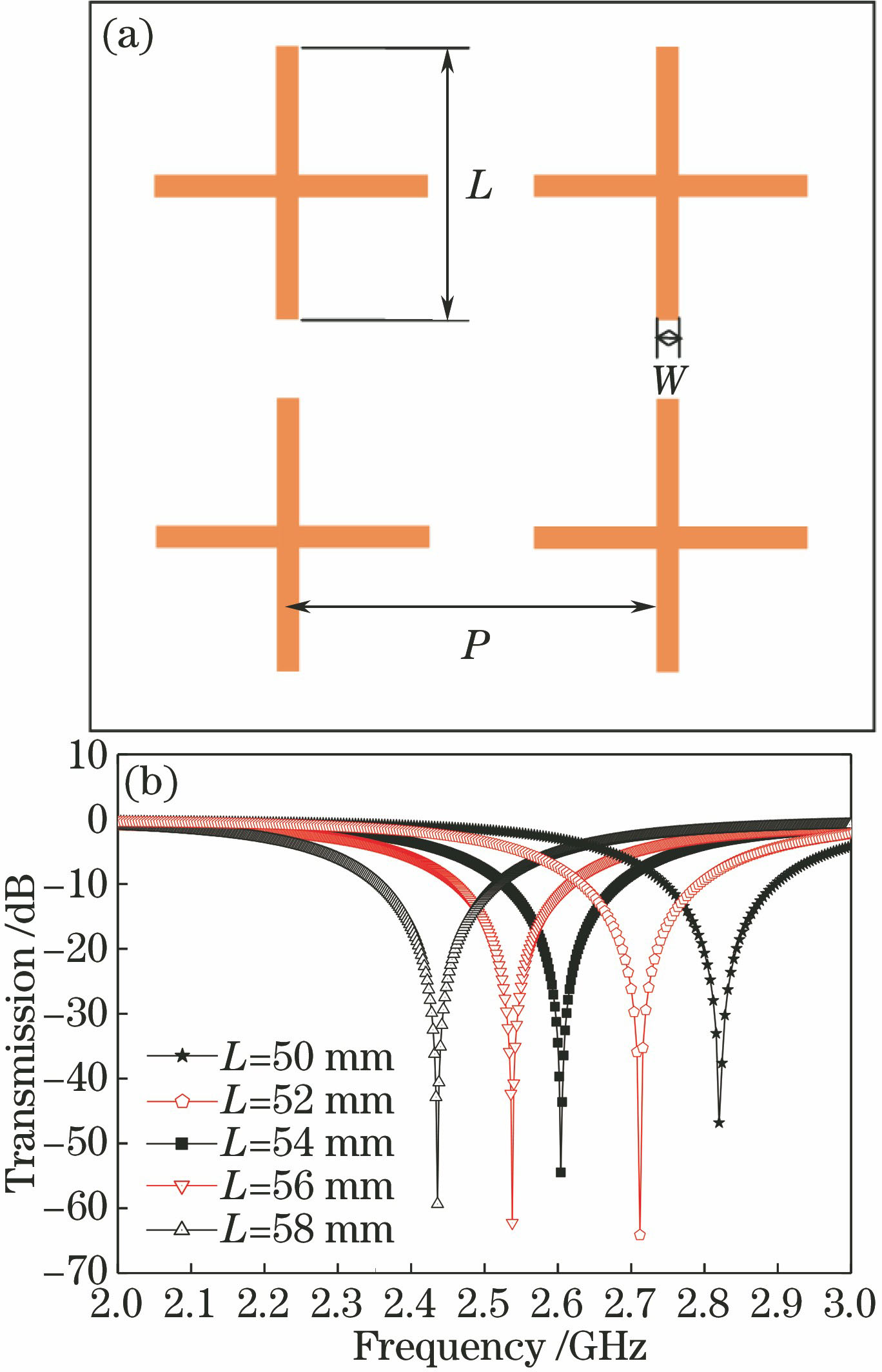
    Fig. 1. Patch element of crossed dipoles. (a) Arrangement of elements; (b) transmission curves with different sizes
    Optically controlled active FSS structure of cross dipole slot-element
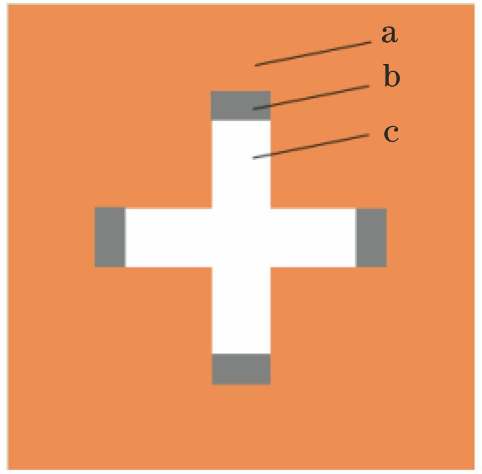
    Fig. 2. Optically controlled active FSS structure of cross dipole slot-element
    Optically controlled active FSS of cross dipole slot-element. (a)Structure size; (b)size and arrangement of elements
    Fig. 3. Optically controlled active FSS of cross dipole slot-element. (a)Structure size; (b)size and arrangement of elements
    Spectra of optically controlled active FSS before and after illumination
    Fig. 4. Spectra of optically controlled active FSS before and after illumination
    Technological process of preparing optically controlled active FSS
    Fig. 5. Technological process of preparing optically controlled active FSS
    Preparation of photoconductive FSS. (a) Coating photoconductive film; (b) spin coating; (c) exposure and development; (d) corrosion; (e) cleaning the photoresist; (f) photo of sample
    Fig. 6. Preparation of photoconductive FSS. (a) Coating photoconductive film; (b) spin coating; (c) exposure and development; (d) corrosion; (e) cleaning the photoresist; (f) photo of sample
    Effect of doping amount of CdSe on spectral response
    Fig. 7. Effect of doping amount of CdSe on spectral response
    Effect of doping mole fraction of Cu on square resistance
    Fig. 8. Effect of doping mole fraction of Cu on square resistance
    Preparation of metal FSS. (a)Spin coating; (b) exposure and development; (c) metal plating; (d) cleaning the photoresist; (e)sample of optically controlled active FSS
    Fig. 9. Preparation of metal FSS. (a)Spin coating; (b) exposure and development; (c) metal plating; (d) cleaning the photoresist; (e)sample of optically controlled active FSS
    Effect of annealing temperature on photoconductive thin film. (a) I-V logarithmic curves at different annealing temperatures; (b) relationship between annealing temperature and film contact square resistance
    Fig. 10. Effect of annealing temperature on photoconductive thin film. (a) I-V logarithmic curves at different annealing temperatures; (b) relationship between annealing temperature and film contact square resistance
    (a) I-V curves at different annealing time; (b) relationship between annealing time and film contact square resistance
    Fig. 11. (a) I-V curves at different annealing time; (b) relationship between annealing time and film contact square resistance
    Bright square resistance of photoconductive thin film irradiated with different frequencies light
    Fig. 12. Bright square resistance of photoconductive thin film irradiated with different frequencies light
    Bright square resistance of photoconductive thin film irradiated with different optical powers
    Fig. 13. Bright square resistance of photoconductive thin film irradiated with different optical powers
    Schematic diagram of the measurement
    Fig. 14. Schematic diagram of the measurement
    Curves of measurement
    Fig. 15. Curves of measurement
    Effect of optical power on shielding
    Fig. 16. Effect of optical power on shielding
    Mole fraction of Cu /%Dark square resistance /(MΩ·□-1)Bright square resistance /(kΩ·□-1)Mole fraction of Cu /%Dark square resistance /(MΩ·□-1)Bright square resistance /(kΩ·□-1)
    01.451.20.007110.03.3
    0.0014.101.40.008162.03.6
    0.00212.41.70.009206.33.9
    0.00318.92.00.010295.04.2
    0.00436.42.40.011371.14.4
    0.00549.82.80.012485.34.8
    0.00678.23.10.013594.25.8
    Table 1. Dark/bright square resistance of photoconductive thin films at different doping amounts for Cu
    Optical power /(mW∙cm-2)Dark square resistance /(MΩ·□-1)Bright square resistance /(kΩ·□-1)
    502910
    100295
    150291
    200290.1
    250290.09
    300290.085
    Table 2. Test results for dark/bright square resistance of photoconductive thin film in different optical powers
    Jun Wang, Yanjun Sun, Xuesong Ji, Li Wang, Yue Wang, Yanbing Leng. Fabrication and Photoelectric Properties of Optically Controlled Active Frequency Selective Surface[J]. Acta Optica Sinica, 2018, 38(5): 0524002
    Download Citation