
Zhen Li, Guanjun Yang. A methylammonium iodide healing method for CH3NH3PbI3 perovskite solar cells with high fill factor over 80%[J]. Journal of Semiconductors, 2021, 42(11): 112202
- Journal of Semiconductors
- Vol. 42, Issue 11, 112202 (2021)
Abstract
1. Introduction
Metal halide perovskites, with formula ABX3, are emerging as a promising photoelectric material owing to their high absorption coefficient, slow carrier recombination and large carrier diffusion lengths[
To realize high-efficiency PSCs, many aspects should be taken into account to reduce the amount of defects that might exist inside the solar cells[
Since the thermal transmission during the stage of the heat treatment is a significant factor that influences the crystallinity and grain size[
Atmosphere healing treatment is also an optional method to improve perovskite film quality[
Herein, we adopt a methylammonium iodide (MAI) healing method to replace the MA gas with the MAI atmosphere in an enclosed space[
2. Material and methods
2.1. Materials
PbI2 (99.99%), MAI (99.5%) and Spiro-MeOTAD (99.8%) were provided by Xi’an Polymer Light Technology Corp. Fluorine-doped tin oxide (FTO)-coated glasses (TEC7, 2.2 mm) were provided by Ying Kou You Xuan Trade Co., Ltd. N,N-dimethylformamide (DMF, anhydrous, 99.8%) was provided by Sigma-Aldrich.
2.2. Film and solar cell fabrication
The acetone, ethanol, and deionized water were used to clean the FTO glasses sequentially, each for 15 min respectively. Afterwards, the FTO glasses were dried by nitrogen and cleaned in UV ozone for 30 min. Then, MAPbI3 precursor (1M) in DMF was spin-coated on the FTO substrate at 2000 rpm for 8 s. Immediately after the spin-coating process, the samples were transferred into a homemade gas-pump device[
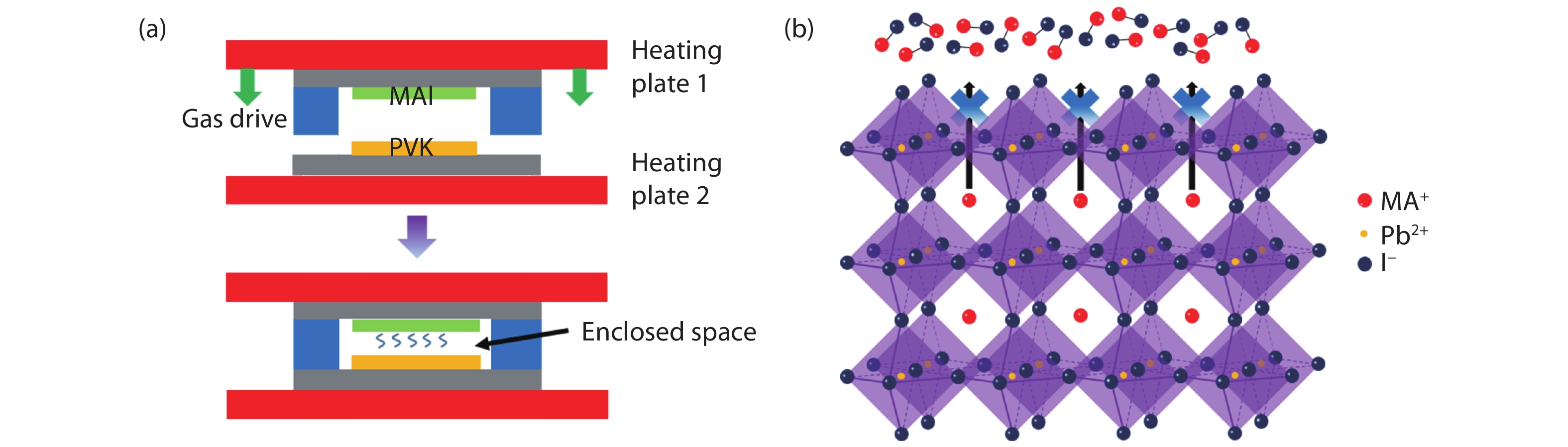
Then, we used a MAI healing method to prevent MAPbI3 material decomposing into PbI2 due to the loss of organic components during the process of heat treatment. The elimination of the PbI2 could remove the obstacle of the grain boundary migration and promote the crystal growth. As shown in Fig. 1(a), MAI and MAPbI3 films were placed on a pair of face-to-face heating plates. Then, the gas-driven heating plates were moved to fit tightly and created an enclosed space. After we elevated the temperature of the heating plates, which were identical for the MAI and MAPbI3 films, the atmosphere rich with MAI molecule could prevent the component loss inside the perovskite films due to the saturation states of the organic ammonium in this enclosed space, as shown in Fig. 1(b).
![]()
Figure 1.(Color online) Schematic diagram of (a) the MAPbI3 perovskite fabrication treated by MAI healing method and (b) MAI healing process.
For PSCs fabrication, a tin dioxide (SnO2) modified titanium dioxide (TiO2) film was fabricated on the FTO substrate according to our previous report[
2.3. Material characterizations
Surface morphology was performed on a field-emission scanning electron microscope (SEM, MIRA3 TESCAN). Roughness of the film surface was tested on a high-resolution atomic force microscopy (AFM, INNOVA). X-ray diffraction (XRD) patterns were tested on an Ultima IV X-ray Diffractometer. Ultraviolet visible (UV–vis) absorption spectra were tested on a PerkinElmer Lambda 950 spectrophotometer. The steady-state photoluminescence (PL) spectra, time-resolution photoluminescence (TRPL) spectra (Excitation wavelength: 375 nm) were performed on a transient steady-state fluorescence spectrometer (Edinburgh FLS9). Photocurrent–voltage (J–V) curves of the PSCs (active area: 0.1 cm2) were studied by a source meter (2400, Keithley). The solar cells were tested with a sweep speed of 0.05 V/s under AM 1.5 G condition of 100 mW/cm2 illumination by using a solar simulator (Peccell Technologies PEC-L01).
3. Results and discussion
3.1. Process parameter optimization
Surface morphology of the MAPbI3 films with different heating temperature and processing time were studied to determine the optimal process parameters of the MAI healing method. The statistics of the grain size in Figs. 2 and 3 showed that increasing the heating temperature and processing time could promote the growth of the perovskite crystal. However, when the heating temperature increased to 150 °C, pinholes started to appear on a large scale and the grain boundary was difficult to distinguish. Moreover, the grain size no longer increased obviously when we extended the processing time from 15 to 18 min. Therefore, the heating temperature and processing time of the MAI healing method were set as 130 °C and 15 min respectively to realize the fabrication of perovskite films in subsequent research.
![]()
Figure 2.(Color online) SEM images of MAPbI3 perovskite treated by MAI healing method with heating temperature of (a) 100 °C, (b) 120 °C, (c) 130 °C and (d) 150 °C. (e) Comparison of grain size of the MAPbI3 film with different heating temperature. (The processing time was set as 10 min.)
![]()
Figure 3.(Color online) SEM images of MAPbI3 perovskite treated by MAI healing method with processing time of (a) 12 min (low magnification), (b) 12 min (high magnification), (c) 15 min and (d) 18 min. (e) Comparison of grain size of the MAPbI3 film with different processing time. (The heating temperature was set as 100 °C.)
3.2. Film quality comparison
To investigate the effect on the surface morphology of the atmosphere healing, the MAPbI3 films were fabricated with the same heating temperature and processing time, which were both treated at 130 °C for 15 min for conventional post-annealing treatment and the MAI healing method. Fig. 4 showed the surface morphology and corresponding statistics of grain size and grain boundary density of the MAPbI3 films fabricated by different treatments. As shown in Figs. 4(a) and 4(b), through the comparison of the SEM images, the MAI healing method is supposed to contribute to the crystal growth, while the film could still keep dense and smooth. Besides, as shown in Figs. 4(c)–4(f), the AFM images also demonstrated that larger grain was realized through the MAI healing method. As shown in Fig. 4(g), according to the results of the corresponding statistics, the average grain size treated by MAI healing method was 880 nm, nearly double that of the film treated by conventional post-annealing. The statistics of grain boundary density in Fig. 4(h) also decreased obviously after the healing process. The much larger grain size should be associated with the atmosphere rich with MAI in the enclosed space, which could repress the decomposition of MAPbI3 and the production of PbI2 around the grain boundaries. Thus, the elimination of the PbI2 obstacle around the grains was supposed to contribute to the perovskite crystal growth.
![]()
Figure 4.(Color online) SEM and AFM images of MAPbI3 perovskite films treated by (a, c, d) post-annealing, (b, e, f) MAI healing. (g) Statistics of the average grain size and (h) grain boundary density of MAPbI3 perovskite film with different treatment.
Fig. 5 showed the XRD patterns and their partial enlarged views of the MAPbI3 films prepared by different heat treatments. The dominant diffraction peaks of the MAPbI3 perovskite were at 2θ = 14.11°, 28.43°, and 31.87°, corresponding to (110) (220) (310) crystal planes respectively, which were identical between these two different treatments. However, the diffraction peak at 2θ = 12.36° of the perovskite film, treated by conventional post-annealing, indicated that a small amount of PbI2 had generated during the heat treatment, while there were no obvious diffraction peaks of PbI2 in the XRD pattern of the perovskite treated by MAI healing method. These results demonstrated that the MAI healing method is an effective way to repress the production of PbI2 during the heat treatment process of MAPbI3 films.
![]()
Figure 5.(Color online) Phase structure of MAPbI3 films with different treatments. (a) XRD patterns. (b) Partial enlarged views.
To further study the absorption and photoluminescence properties, we tested the UV–vis, PL and TRPL spectra of the MAPbI3 films prepared by different treatment. The absorbance of the MAPbI3 films treated by MAI healing was higher than that of the film treated by post-annealing due to reduced grain boundaries, where the light scattering usually happens, as shown in Fig. 6(a). Besides, we exposed a sample treated by MAI healing under ambient condition (relative humidity: 30%–40%) for 10 days. The absorption intensity kept steady during this testing period, indicating the perovskite film possessed an excellent stability, as shown in Fig. 6(b).
![]()
Figure 6.(Color online) Optical and electrical spectra of MAPbI3 films with different treatments. (a) UV–vis spectra of MAPbI3 film with different treatments. (b) UV–vis spectra of MAPbI3 film treated by MAI healing as-prepared and after storage in ambient air (relative humidity: 30%–40%) for 10 days. (c) PL and (d) TRPL spectra of MAPbI3 films with different treatment.
PL spectra were also tested to further investigate the photoluminescence properties. Fig. 6(c) showed that the emission peaks were both located at 770 nm, while the PL intensity of MAPbI3 films treated by the MAI healing method was much higher than that of the MAPbI3 films treated by conventional post-annealing. Moreover, TRPL measurements in Fig. 6(d) showed that the MAPbI3 perovskite film treated by the MAI healing method had a significantly longer average lifetime of 93.5 ns, while that of the MAPbI3 perovskite film treated by conventional post-annealing was only 40.8 ns.
3.3. Photovoltaic performance and stability
PSCs in a n–i–p configuration were fabricated to evaluate the photovoltaic performance and stability of the PSCs prepared by post-annealing and MAI healing treatment. The cross section SEM image in Fig. 7(a) demonstrated that a vertical columnar grain layer of perovskite was formed via the MAI healing treatment. Fig. 7(b) showed that the best device treated by the MAI healing method obtained a PCE of 18.89% with an open-circuit voltage (Voc) of 1.05 V, a short-circuit current density (Jsc) of 21.98 mA/cm2, and an FF of 81.6%. The value of FF was much higher than most of the MAPbI3-based PSCs without any additive or post-treatment, indicating that the MAI healing method was an effective way to increase the FF of the PSCs based on the MAPbI3 absorber. For comparison, the best device treated by conventional post-annealing obtained a PCE of 18.4% with a Voc of 1.08 V, a Jsc of 21.28 mA/cm2, and an FF of 79.9%, respectively. The average statistical results in Table 1 indicated that the MAI healing method could improve the PCE by nearly 1% compared with the devices treated by conventional post-annealing. A lower current loss due to the reduced defects inside the PSCs was supposed to contribute to the evidently enhanced Jsc and FF.
![]()
Figure 7.(Color online) (a) Cross section SEM image of the PSCs treated by MAI healing. (b)
Furthermore, we recorded the photovoltaic performance of the PSCs treated by post-annealing and the MAI healing method as-prepared and after storage under ambient conditions (relative humidity: 30%–40%) for 192 h continuously. As shown inFig. 7(c), the Voc for both of the devices remained steady, while the Jsc and FF of the device treated by conventional post-annealing dropped significantly during this period, causing the PCE to decrease to less than 60% of the initial state. In contrast, the device treated by the MAI healing method still retained 90% of its initial PCE after the testing period, showing outstanding humidity stability.
4. Conclusion
In conclusion, we used a MAI healing method to prevent the decomposition of MAPbI3 and the production of PbI2 during the heat treatment. Through the healing treatment, a larger grain size over 800 nm was successfully realized. Moreover, the absorption and photoluminescence intensity were both improved obviously in comparison with the conventional post-annealing treatment. Finally, the best PCE of 18.89% with an ultrahigh FF over 80% was realized in an n–i–p configuration via the healing method, while retaining 90% of its initial state after storage in ambient conditions for 192 h continuously. This work indicates that adopting the MAI healing method to repress the volatilization process of the organic component during heat treatment contributes to the films quality, photovoltaic performance and humidity stability of the MAPbI3-based PSCs. The application of this healing method in other perovskite compositions should be studied in the future.
Acknowledgements
This work was fianancially supported by the National Key R&D Program of China (Grant No. 2019YFB1503200). We thank Dr. Ying Hao and Dr. Lu Bai for their kind assistance in UV–vis spectra tests.
References
[1] C T Zuo, H J Bolink, H W Han et al. Advances in perovskite solar cells. Adv Sci, 3, 1500324(2016).
[2] A K Jena, A Kulkarni, T Miyasaka. Halide perovskite photovoltaics: background, status, and future prospects. Chem Rev, 119, 3036(2019).
[3] J Y Kim, J W Lee, H S Jung et al. High-efficiency perovskite solar cells. Chem Rev, 120, 7867(2020).
[4] P Wang, Y H Wu, B Cai et al. Solution-processable perovskite solar cells toward commercialization: progress and challenges. Adv Funct Mater, 29, 1807661(2019).
[5] F Huang, M J Li, P Siffalovic et al. From scalable solution fabrication of perovskite films towards commercialization of solar cells. Energy Environ Sci, 12, 518(2019).
[6] A Kojima, K Teshima, Y Shirai et al. Organometal halide perovskites as visible-light sensitizers for photovoltaic cells. J Am Chem Soc, 131, 6050(2009).
[7] J Jeong, M Kim, J Seo et al. Pseudo-halide anion engineering for α-FAPbI3 perovskite solar cells. Nature, 592, 381(2021).
[8] S G Motti, D Meggiolaro, S Martani et al. Defect activity in lead halide perovskites. Adv Mater, 31, 1901183(2019).
[9] A F Castro-Méndez, J Hidalgo, J P Correa-Baena. The role of grain boundaries in perovskite solar cells. Adv Energy Mater, 9, 1901489(2019).
[10] Y Q Yang, J H Wu, X B Wang et al. Suppressing vacancy defects and grain boundaries via ostwald ripening for high-performance and stable perovskite solar cells. Adv Mater, 32, 1904347(2020).
[11] W C Kong, S W Wang, F Li et al. Ultrathin perovskite monocrystals boost the solar cell performance. Adv Energy Mater, 10, 2000453(2020).
[12] C T Zuo, L M Ding. An 80.11% FF record achieved for perovskite solar cells by using the NH4Cl additive. Nanoscale, 6, 9935(2014).
[13] S R Wang, A L Wang, X Y Deng et al. Lewis acid/base approach for efficacious defect passivation in perovskite solar cells. J Mater Chem A, 8, 12201(2020).
[14] S B Xiong, T Y Hao, Y Y Sun et al. Defect passivation by nontoxic biomaterial yields 21% efficiency perovskite solar cells. J Energy Chem, 55, 265(2021).
[15] F Zhang, K Zhu. Additive engineering for efficient and stable perovskite solar cells. Adv Energy Mater, 10, 1902579(2020).
[16] L S Xie, Z Y Cao, J W Wang et al. Improving energy level alignment by adenine for efficient and stable perovskite solar cells. Nano Energy, 74, 104846(2020).
[17] J Z Chen, N G Park. Materials and methods for interface engineering toward stable and efficient perovskite solar cells. ACS Energy Lett, 5, 2742(2020).
[18] S H Chin, J W Choi, H C Woo et al. Realizing a highly luminescent perovskite thin film by controlling the grain size and crystallinity through solvent vapour annealing. Nanoscale, 11, 5861(2019).
[19] B B Liu, S Wang, Z R Ma et al. High-performance perovskite solar cells with large grain-size obtained by the synergy of urea and dimethyl sulfoxide. Appl Surf Sci, 467/468, 708(2019).
[20] S Kavadiya, J Strzalka, D M Niedzwiedzki et al. Crystal reorientation in methylammonium lead iodide perovskite thin film with thermal annealing. J Mater Chem A, 7, 12790(2019).
[21] C T Zuo, L M Ding. Drop-casting to make efficient perovskite solar cells under high humidity. Angew Chem Int Ed, 60, 1(2021).
[22] X D Ren, Z Yang, D Yang et al. Modulating crystal grain size and optoelectronic properties of perovskite films for solar cells by reaction temperature. Nanoscale, 8, 3816(2016).
[23] C C Boyd, R Cheacharoen, T Leijtens et al. Understanding degradation mechanisms and improving stability of perovskite photovoltaics. Chem Rev, 119, 3418(2019).
[24] J Bisquert, E J Juarez-Perez. The causes of degradation of perovskite solar cells. J Phys Chem Lett, 10, 5889(2019).
[25] S P Dunfield, L Bliss, F Zhang et al. From defects to degradation: a mechanistic understanding of degradation in perovskite solar cell devices and modules. Adv Energy Mater, 10, 1904054(2020).
[26] B Shi, X Yao, F H Hou et al. Unraveling the passivation process of PbI2 to enhance the efficiency of planar perovskite solar cells. J Phys Chem C, 122, 21269(2018).
[27] Y C Chen, Q Meng, Y Y Xiao et al. Mechanism of PbI2 in situ passivated perovskite films for enhancing the performance of perovskite solar cells. ACS Appl Mater Interfaces, 11, 44101(2019).
[28] X J Huang, G P Dong, L M Ding. The recovery of perovskites. Sci Bull, 65, 1600(2020).
[29] Z M Zhou, Z W Wang, Y Y Zhou et al. Methylamine-gas-induced defect-healing behavior of CH3NH3PbI3 thin films for perovskite solar cells. Angew Chem Int Ed, 54, 9705(2015).
[30] C W Li, S P Pang, H X Xu et al. Methylamine gas based synthesis and healing process toward upscaling of perovskite solar cells: progress and perspective. Sol RRL, 1, 1700076(2017).
[31]
[32] B Ding, L L Gao, L S Liang et al. Facile and scalable fabrication of highly efficient lead iodide perovskite thin-film solar cells in air using gas pump method. ACS Appl Mater Interfaces, 8, 20067(2016).
[33] B Ding, S Y Huang, Q Q Chu et al. Low-temperature SnO2-modified TiO2 yields record efficiency for normal planar perovskite solar modules. J Mater Chem A, 6, 10233(2018).

Set citation alerts for the article
Please enter your email address
© Copyright 2018-2021 | Chinese Laser Press. All Rights Reserved 沪ICP备15018463号-20