Shihao Liu, Letian Zhang, Wenfa Xie. Solution processed organic light-emitting devices: structure, device physics and fabrication process[J]. Opto-Electronic Engineering, 2022, 49(5): 210407
Search by keywords or author
- Opto-Electronic Engineering
- Vol. 49, Issue 5, 210407 (2022)
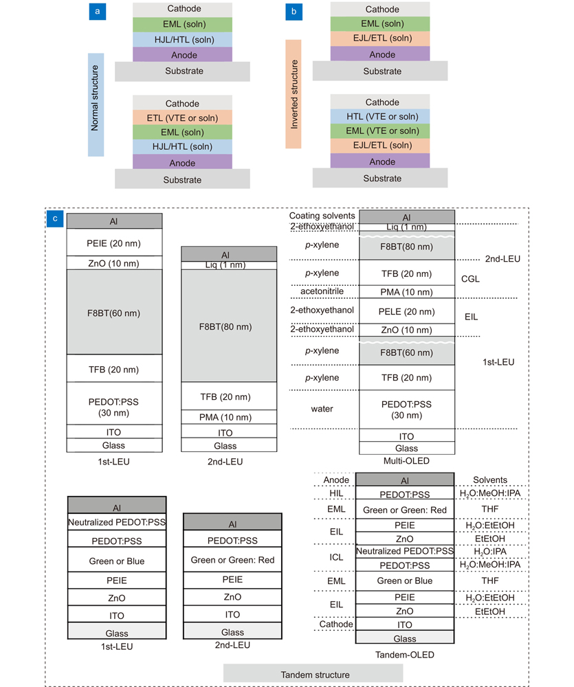
![Schematic diagrams of device structures of solution-processed OLEDs.(a) Normal structure; (b) Inverted structure; (c) Tandem structure. Soln and VTE in bracket respectivelyrepresent solution-processed and thermally evaporated under high vacuum[30-31]](/richHtml/gdgc/2022/49/5/210407/1_210407-1.jpg)
Fig. 1. Schematic diagrams of device structures of solution-processed OLEDs.
(a) Normal structure; (b) Inverted structure; (c) Tandem structure. Soln and VTE in bracket respectively
represent solution-processed and thermally evaporated under high vacuum[30-31]
![Schematic diagrams of current balance in hole-dominated OLEDs.(a) A case of ETL without hole blocking; (b) A case of ETL with hole blocking; (c) Energy levels and capacitance-voltage-current density characteristics of two hole-dominated OLEDs [52]](/richHtml/gdgc/2022/49/5/210407/1_210407-2.jpg)
Fig. 2. Schematic diagrams of current balance in hole-dominated OLEDs.
(a) A case of ETL without hole blocking; (b) A case of ETL with hole blocking;
(c) Energy levels and capacitance-voltage-current density characteristics of two hole-dominated OLEDs [52]
Fig. 3. (a) Schematic diagram of SPP at metal-dielectric surface; (b) Power dissipation spectra of dipole radiation. TMv, TMh and TEh respectively represent TM mode from vertical dipole, TM mode and TE mode from horizontal dipole[14]; (c) Optical power modal analysis vs ETL thickness of a conventional OLED. The power is distributed into air (Air), substrate (Sub), waveguide (WV), surface plasmon polariton (SPP) and lossy metal (Loss) modes[56]
Fig. 4. Schematic diagram of solution-processing technologies. (a) Spin coating process; (b) Ultrasonic spray coating process [64]; (c) Blade coating process; (d) Inkjet printing process

Set citation alerts for the article
Please enter your email address


