• Photonics Research
  • Vol. 8, Issue 4, 564 (2020)
Yuan Meng1、2、†, Zhoutian Liu1、3、†, Zhenwei Xie4, Ride Wang5, Tiancheng Qi1、3, Futai Hu1, Hyunseok Kim2、6, Qirong Xiao1、3、*, Xing Fu1、3, Qiang Wu5, Sang-Hoon Bae2、6, Mali Gong1、3、7, and Xiaocong Yuan4
Author Affiliations
  • 1State Key Laboratory of Precision Measurement Technology and Instruments, Department of Precision Instrument, Tsinghua University, Beijing 100084, China
  • 2Research Laboratory of Electronics, Massachusetts Institute of Technology, Cambridge, Massachusetts 02139, USA
  • 3Key Laboratory of Photonic Control Technology, Ministry of Education, Tsinghua University, Beijing 100084, China
  • 4Nanophotonics Research Centre, Shenzhen Key Laboratory of Micro-Scale Optical Information Technology, Shenzhen University, Shenzhen 518060, China
  • 5Key Laboratory of Weak-Light Nonlinear Photonics, Ministry of Education, TEDA Institute of Applied Physics and School of Physics, Nankai University, Tianjin 300457, China
  • 6Department of Mechanical Engineering, Massachusetts Institute of Technology, Cambridge, Massachusetts 02139, USA
  • 7e-mail: gongml@mail.tsinghua.edu.cn
  • show less
    DOI: 10.1364/PRJ.384449 Cite this Article Set citation alerts
    Yuan Meng, Zhoutian Liu, Zhenwei Xie, Ride Wang, Tiancheng Qi, Futai Hu, Hyunseok Kim, Qirong Xiao, Xing Fu, Qiang Wu, Sang-Hoon Bae, Mali Gong, Xiaocong Yuan. Versatile on-chip light coupling and (de)multiplexing from arbitrary polarizations to controlled waveguide modes using an integrated dielectric metasurface[J]. Photonics Research, 2020, 8(4): 564 Copy Citation Text show less
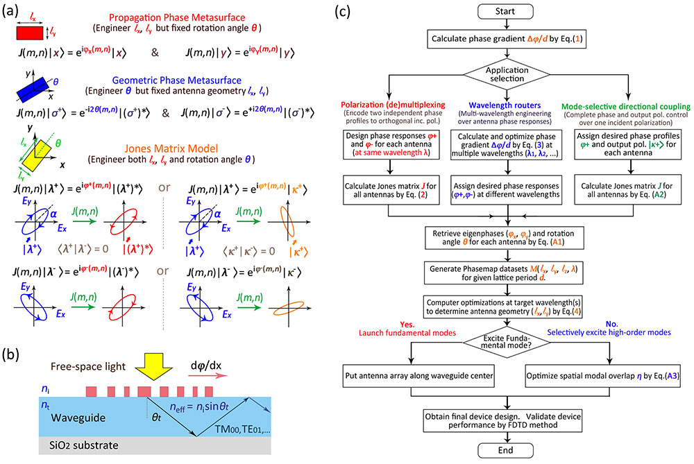
    (a) Metasurface concepts comparison. Propagation phase metasurface: engineered antenna geometry (lx,ly) but fixed rotation angle θ. Geometric phase metasurface: identical antennas with spatially varying orientation angle [3941" target="_self" style="display: inline;">–41]. In the Jones matrix model (two working scenarios), red or orange color-highlighted phases or polarizations represent configurable parameters, while black or gray colored parts denote given or not configurable factors. (b) The normally incident light can be directionally coupled into specific waveguide modes after consecutive interactions with the gradient metasurface. (c) Flow chart for design process (detailed in Methods section).
    Fig. 1. (a) Metasurface concepts comparison. Propagation phase metasurface: engineered antenna geometry (lx,ly) but fixed rotation angle θ. Geometric phase metasurface: identical antennas with spatially varying orientation angle [3941" target="_self" style="display: inline;">–41]. In the Jones matrix model (two working scenarios), red or orange color-highlighted phases or polarizations represent configurable parameters, while black or gray colored parts denote given or not configurable factors. (b) The normally incident light can be directionally coupled into specific waveguide modes after consecutive interactions with the gradient metasurface. (c) Flow chart for design process (detailed in Methods section).
    Polarization (de)multiplexers for arbitrary elliptical polarizations. (a), (e), and (i) Device structure sketch for splitting arbitrary orthogonal polarizations (|λ+⟩=R(π/4)·[cos(ε)|x⟩+i×sin(ε)|y⟩], |λ−⟩=R(π/4)·[i×sin(ε)|x⟩+cos(ε)|y⟩]) with three representative incident elliptical parameters ε=40°, 60°, and 80°, respectively. Accompanied forms: antenna design details (fixed antenna height: lz=1.2 μm). (b), (f), and (j) Corresponding incident polarization illustrations. (c), (g), and (k) Coupling efficiency as a function of wavelength for ε=40°, 60°, and 80°, respectively, validating that our method is applicable for arbitrary polarizations. (d), (h), and (l) Corresponding directivity spectra.
    Fig. 2. Polarization (de)multiplexers for arbitrary elliptical polarizations. (a), (e), and (i) Device structure sketch for splitting arbitrary orthogonal polarizations (|λ+=R(π/4)·[cos(ε)|x+i×sin(ε)|y], |λ=R(π/4)·[i×sin(ε)|x+cos(ε)|y]) with three representative incident elliptical parameters ε=40°, 60°, and 80°, respectively. Accompanied forms: antenna design details (fixed antenna height: lz=1.2  μm). (b), (f), and (j) Corresponding incident polarization illustrations. (c), (g), and (k) Coupling efficiency as a function of wavelength for ε=40°, 60°, and 80°, respectively, validating that our method is applicable for arbitrary polarizations. (d), (h), and (l) Corresponding directivity spectra.
    (a) Device schematic of the integrated linear-polarization (de)multiplexer. Waveguide width×height=680 nm×600 nm. (b) Phase map showing the phase retardation of transmitted light as a function of antenna geometry (lx,ly) at λ=1.55 μm with fixed antenna height lz=1.2 μm. (c) Distribution of electric field component Ey in the x–y plane under |y⟩ plane wave illumination (λ=1.55 μm). Antenna and waveguide profiles are marked in solid and dashed lines, respectively. (d), (e) Full-wave simulations showing the directional coupling of electric field components Ez and Ey into opposite directions under illumination of linear |x⟩ and |y⟩ polarizations, respectively. (f), (g) Vector diagram of the electric field at the left (under |x⟩ illumination) and right (|y⟩ illumination) waveguide ports , respectively, at λ=1.55 μm. (h) Corresponding electric field norm |E| distribution. (i), (j) Coupling efficiency spectra under |x⟩ and |y⟩ excitations, respectively. (k) Structure sketch for the circular-polarization (de)multiplexer. (l) Circular polarization demultiplexing: |E| distributions under incident left-handed (LCP) and right-handed circular polarization (RCP). (m) Vector diagram and |E| distribution at the right waveguide port (approximate TM00 mode) under LCP incidence (λ=1.55 μm). (n) Coupling efficiency spectrum (LCP illumination). (o) Directivity spectrum.
    Fig. 3. (a) Device schematic of the integrated linear-polarization (de)multiplexer. Waveguide width×height=680  nm×600  nm. (b) Phase map showing the phase retardation of transmitted light as a function of antenna geometry (lx,ly) at λ=1.55  μm with fixed antenna height lz=1.2  μm. (c) Distribution of electric field component Ey in the xy plane under |y plane wave illumination (λ=1.55  μm). Antenna and waveguide profiles are marked in solid and dashed lines, respectively. (d), (e) Full-wave simulations showing the directional coupling of electric field components Ez and Ey into opposite directions under illumination of linear |x and |y polarizations, respectively. (f), (g) Vector diagram of the electric field at the left (under |x illumination) and right (|y illumination) waveguide ports , respectively, at λ=1.55  μm. (h) Corresponding electric field norm |E| distribution. (i), (j) Coupling efficiency spectra under |x and |y excitations, respectively. (k) Structure sketch for the circular-polarization (de)multiplexer. (l) Circular polarization demultiplexing: |E| distributions under incident left-handed (LCP) and right-handed circular polarization (RCP). (m) Vector diagram and |E| distribution at the right waveguide port (approximate TM00 mode) under LCP incidence (λ=1.55  μm). (n) Coupling efficiency spectrum (LCP illumination). (o) Directivity spectrum.
    (a) Structure for the multifunctional (de)multiplexer for circular polarizations. When working at a fixed wavelength, it functions as a spin/polarization demultiplexer, while under fixed incident polarizations it works as a wavelength demultiplexer/color router. (b), (c) Coupling efficiency spectrum under LCP and RCP illumination, respectively. (d)–(f) Similar to (a)–(c) but for device working for linear polarizations. The shape difference between the curves in (e) and (f) can be ascribed to the discrepancy of spatial modal overlap η under different incident polarizations.
    Fig. 4. (a) Structure for the multifunctional (de)multiplexer for circular polarizations. When working at a fixed wavelength, it functions as a spin/polarization demultiplexer, while under fixed incident polarizations it works as a wavelength demultiplexer/color router. (b), (c) Coupling efficiency spectrum under LCP and RCP illumination, respectively. (d)–(f) Similar to (a)–(c) but for device working for linear polarizations. The shape difference between the curves in (e) and (f) can be ascribed to the discrepancy of spatial modal overlap η under different incident polarizations.
    (a) Device structure sketch for the waveguide-integrated mode-selective directional coupler. A left single-row antenna array (namely TE00 antennas) is applied to excite left-propagating TE00 mode. Double rows of identical antenna arrays (namely TE10 antennas) with dislocations of Δx≈0.5 μm in the x direction and Δy≈0.8 μm in the y direction. Accompanied form: detailed design parameters. (b) Electric field component Ey distribution along middle waveguide plane under the illumination of |y⟩ polarized plane wave. (c) Antenna near fields (see Methods). Left and middle panels: Ey and Ex distributions for an lx×ly=0.2 μm×0.4 μm antenna (θ = 0°) placed at waveguide center (as TE00 antennas). Right panel: Ez distribution along the center plane between two TE10 antennas (m=−4 for upper and lower groups). (d) Electric field distributions for ideal TE00 (Ey), TM00 (Ex), and TE10 (Ey) modes. (e) Calculated output |Ey| distributions for the left (upper panel) and right (lower panel) waveguide ports accordingly. (f) Corresponding vector diagram of output electric fields at waveguide ports, agreeing well with TE00 and TE10 modes. (g) Device structure (with antenna design parameters) launching left-propagating TM11 mode with two rows of dislocated antennas (upper and lower groups). Right panel: simulated output |Ez| distribution at the left waveguide port at λ=1.55 μm. (h) Design schematic for the directional coupler to selectively excite TM20 mode (with three antenna rows). Antenna center coordinates: ymid=0, yup=−ylow=0.7 μm. Right panel: |Ez| distribution at the left waveguide port (λ=1.55 μm).
    Fig. 5. (a) Device structure sketch for the waveguide-integrated mode-selective directional coupler. A left single-row antenna array (namely TE00 antennas) is applied to excite left-propagating TE00 mode. Double rows of identical antenna arrays (namely TE10 antennas) with dislocations of Δx0.5  μm in the x direction and Δy0.8  μm in the y direction. Accompanied form: detailed design parameters. (b) Electric field component Ey distribution along middle waveguide plane under the illumination of |y polarized plane wave. (c) Antenna near fields (see Methods). Left and middle panels: Ey and Ex distributions for an lx×ly=0.2  μm×0.4  μm antenna (θ = 0°) placed at waveguide center (as TE00 antennas). Right panel: Ez distribution along the center plane between two TE10 antennas (m=4 for upper and lower groups). (d) Electric field distributions for ideal TE00 (Ey), TM00 (Ex), and TE10 (Ey) modes. (e) Calculated output |Ey| distributions for the left (upper panel) and right (lower panel) waveguide ports accordingly. (f) Corresponding vector diagram of output electric fields at waveguide ports, agreeing well with TE00 and TE10 modes. (g) Device structure (with antenna design parameters) launching left-propagating TM11 mode with two rows of dislocated antennas (upper and lower groups). Right panel: simulated output |Ez| distribution at the left waveguide port at λ=1.55  μm. (h) Design schematic for the directional coupler to selectively excite TM20 mode (with three antenna rows). Antenna center coordinates: ymid=0, yup=ylow=0.7  μm. Right panel: |Ez| distribution at the left waveguide port (λ=1.55  μm).
    (a) Device schematic for chip-integrated OAM generator: directional coupling normally incident linearly y-polarized plane wave into right-propagating optical vortex beam. (b) Top view of the device with design parameters manifested in the accompanied forms. Δx2≈0.415 μm and Δy≈0.8 μm. (c) Working principle illustration: combining TE01 and TE10 modes with π/2 phase difference can theoretically produce a helically phased vortex field with topological charge ℓ=+1. Upper panels: |Ey| distributions for ideal TE01, TE10 and mixed OAM modes accordingly. Lower panels: corresponding phase distributions. (d) Calculated output electric field |Ey| distributions when only the TE01 antennas exist (left panel), only TE10 antennas exist (middle panel), and both TE01 and TE10 antennas exist (right panels). Right most panel: corresponding (to the right panel) phase distribution at waveguide right port showing OAM+1 mode. White lines denote waveguide profile. (e), (f) Coupling efficiency and mode purity spectra when only the TE01 (left panel) or TE10 (right panel) antennas are present accordingly. (g) Calculated output OAM−1 mode [|Ey| and phase (|Ey|)] distributions after re-arranging the relative locations of the TE01 and TE10 antennas in the x direction. (h), (i) Output vortex beam [instantaneous Ey and phase (Ey) at λ=1.45 μm] with ℓ=+1 and ℓ=−1, respectively, after exiting waveguide right port with a propagation distance of 2 μm in free space.
    Fig. 6. (a) Device schematic for chip-integrated OAM generator: directional coupling normally incident linearly y-polarized plane wave into right-propagating optical vortex beam. (b) Top view of the device with design parameters manifested in the accompanied forms. Δx20.415  μm and Δy0.8  μm. (c) Working principle illustration: combining TE01 and TE10 modes with π/2 phase difference can theoretically produce a helically phased vortex field with topological charge =+1. Upper panels: |Ey| distributions for ideal TE01, TE10 and mixed OAM modes accordingly. Lower panels: corresponding phase distributions. (d) Calculated output electric field |Ey| distributions when only the TE01 antennas exist (left panel), only TE10 antennas exist (middle panel), and both TE01 and TE10 antennas exist (right panels). Right most panel: corresponding (to the right panel) phase distribution at waveguide right port showing OAM+1 mode. White lines denote waveguide profile. (e), (f) Coupling efficiency and mode purity spectra when only the TE01 (left panel) or TE10 (right panel) antennas are present accordingly. (g) Calculated output OAM1 mode [|Ey| and phase (|Ey|)] distributions after re-arranging the relative locations of the TE01 and TE10 antennas in the x direction. (h), (i) Output vortex beam [instantaneous Ey and phase (Ey) at λ=1.45  μm] with =+1 and =1, respectively, after exiting waveguide right port with a propagation distance of 2 μm in free space.
    Analysis on the impact of different light sources for the device in Fig. 4(a). (a)–(c) Coupling efficiency spectrum under the excitation of different (RCP) light sources: (a) diffracting plane wave (plane wave trimmed by a rectangular aperture: x×y=8 μm×0.6 μm); (b), (c) focused Gaussian beams by a thin lens with circular (lens numerical aperture NA=0.2) and elliptical light spot (after beam transformation with lens NA=0.6), respectively. Insets: illumination condition sketch showing the relative size of the light spot and antenna array (see Methods). (d) Comparison of coupling directivity spectra.
    Fig. 7. Analysis on the impact of different light sources for the device in Fig. 4(a). (a)–(c) Coupling efficiency spectrum under the excitation of different (RCP) light sources: (a) diffracting plane wave (plane wave trimmed by a rectangular aperture: x×y=8  μm×0.6  μm); (b), (c) focused Gaussian beams by a thin lens with circular (lens numerical aperture NA=0.2) and elliptical light spot (after beam transformation with lens NA=0.6), respectively. Insets: illumination condition sketch showing the relative size of the light spot and antenna array (see Methods). (d) Comparison of coupling directivity spectra.
    (a) Illustration of fabrication (fab) error on antenna geometry. (b)–(d) Coupling efficiency spectra for device shown in Fig. 3(a) with random (independent) fabrication errors Δlx, Δly obeying normal distributions ∼N(0,102), N(0,202), and N(5,102), respectively. (e) Comparison of directivity spectrum. (f) Sketch of an antenna cell with random fabrication error on geometry (Δlx,Δly, unit: nm) and rotation angle (Δθ, unit: °). (g)–(i) Coupling efficiency curves for the device in Fig. 3(k) with (g) Δlx,Δly∼N(0,102), (h) Δlx,Δly∼N(0,202), and (i) Δθ∼N(0,102), respectively. (j) Directivity comparison. (k) Misalignment illustration of the whole antenna array(s) on a waveguide with positive Δym. (l), (m) Coupling efficiency spectra for the device in Fig. 4(a) with misalignments Δym=+100 nm and −100 nm, respectively. (n), (o) Comparisons of directivity spectra for the devices in Figs. 3(a) and 5(a) with different values of Δym.
    Fig. 8. (a) Illustration of fabrication (fab) error on antenna geometry. (b)–(d) Coupling efficiency spectra for device shown in Fig. 3(a) with random (independent) fabrication errors Δlx, Δly obeying normal distributions N(0,102), N(0,202), and N(5,102), respectively. (e) Comparison of directivity spectrum. (f) Sketch of an antenna cell with random fabrication error on geometry (Δlx,Δly, unit: nm) and rotation angle (Δθ, unit: °). (g)–(i) Coupling efficiency curves for the device in Fig. 3(k) with (g) Δlx,ΔlyN(0,102), (h) Δlx,ΔlyN(0,202), and (i) ΔθN(0,102), respectively. (j) Directivity comparison. (k) Misalignment illustration of the whole antenna array(s) on a waveguide with positive Δym. (l), (m) Coupling efficiency spectra for the device in Fig. 4(a) with misalignments Δym=+100  nm and 100  nm, respectively. (n), (o) Comparisons of directivity spectra for the devices in Figs. 3(a) and 5(a) with different values of Δym.
    Yuan Meng, Zhoutian Liu, Zhenwei Xie, Ride Wang, Tiancheng Qi, Futai Hu, Hyunseok Kim, Qirong Xiao, Xing Fu, Qiang Wu, Sang-Hoon Bae, Mali Gong, Xiaocong Yuan. Versatile on-chip light coupling and (de)multiplexing from arbitrary polarizations to controlled waveguide modes using an integrated dielectric metasurface[J]. Photonics Research, 2020, 8(4): 564
    Download Citation