
Xiaohui Yang, Qi Wang, Zewu Xiao, Xiaoyan Wu, Jie Ren, Yanting Wu. Highly Efficient Green-Emitting Devices Based on Mixed-Cation Perovskites[J]. Acta Optica Sinica, 2019, 39(10): 1016002
- Acta Optica Sinica
- Vol. 39, Issue 10, 1016002 (2019)
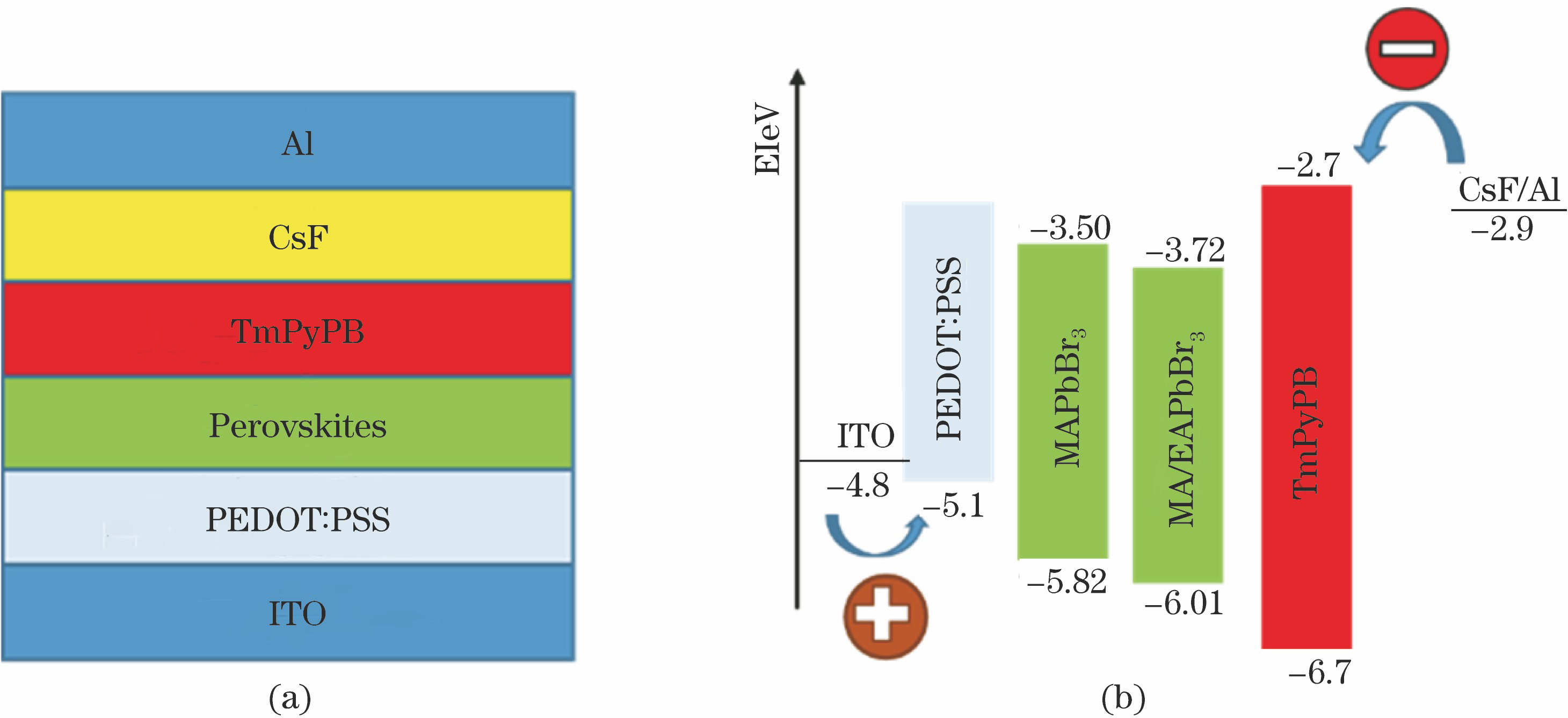
Fig. 1. Configuration and energy level diagram of light-emitting devices. (a) Configuration; (b) energy level
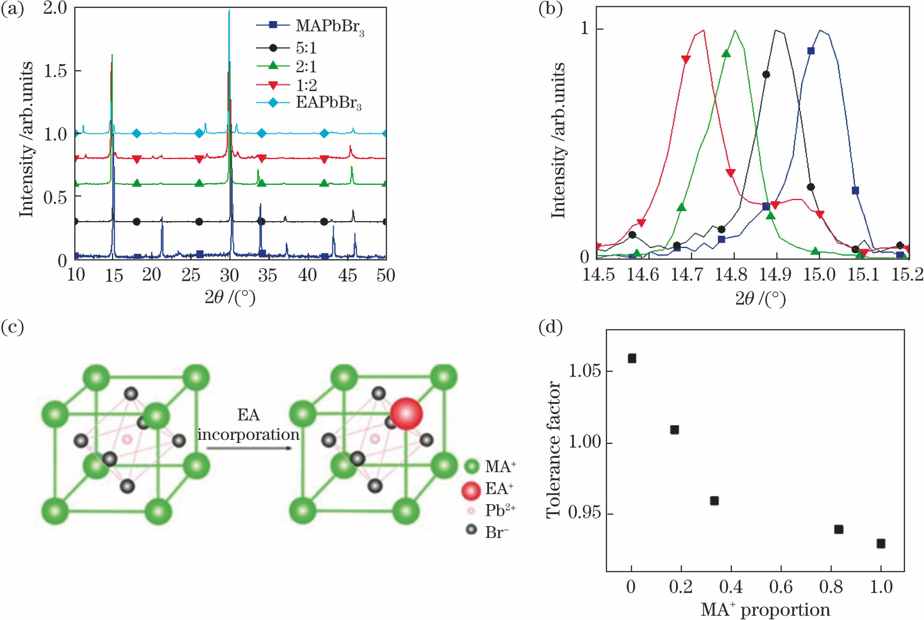
Fig. 2. Crystal structures of perovskite materials. (a) XRD patterns; (b) enlarged version of the (100) diffraction peak region; (c) substitution of MA+ in the MAPbBr3 core by EA+; (d) tolerance factor of MAx EA(1-x )PbBr3 as a function of the MA+ proportion
Fig. 3. Morphologies of perovskite samples (intest show high-resolution SEM images). (a) MAPbBr3, top-view; (b) 5∶1 sample, top-view; (c) 2∶1 sample, top-view; (d) 1∶2 sample, top-view; (e) cross-sectional SEM image of the 2∶1 sample
Fig. 4. Photo-physics properties of the perovskite samples. (a) UV-vis absorption spectra; (b) steady-state PL spectra, insets show the images of the 2∶1 sample under white (left) and UV light (right); the MAPbBr3 and 2∶1 samples for (c) UPS spectra, (d) time-resolved luminescence decay curves, (e) I -V characteristics of hole-dominated devices, and (f) photo-stability measurements
Fig. 5. Properties of light-emitting devices. (a) J-L-V characteristics; (b) EQE-voltage curves; (c) power efficiency-voltage plots; (d) EL spectra, inset is a photo of 2 ∶1 device; (e) operational stability measurements of the MAPbBr3 and 2∶1 devices
|
Table 1. Fitting parameters of the time-resolved luminescence decay characteristics of the samples
|
Table 2. Detailed properties of light-emitting devices

Set citation alerts for the article
Please enter your email address
© Copyright 2018-2021 | Chinese Laser Press. All Rights Reserved 沪ICP备15018463号-20