Author Affiliations
1Photonics Research Institute, Department of Electrical Engineering, The Hong Kong Polytechnic University, Kowloon, Hong Kong, China2Department of Electrical Engineering, Centre for Biosystems, Neuroscience, and Nanotechnology, City University of Hong Kong, Kowloon, Hong Kong, China3State Key Laboratory of Terahertz and Millimeter Waves, City University of Hong Kong, Kowloon, Hong Kong, China4Photonics Research Institute, Department of Electronic and Information Engineering, The Hong Kong Polytechnic University, Kowloon, Hong Kong, China5e-mail: yaoliang@m.scnu.edu.cn6e-mail: dptsai@cityu.edu.hk7e-mail: changyuan.yu@polyu.edu.hkshow less
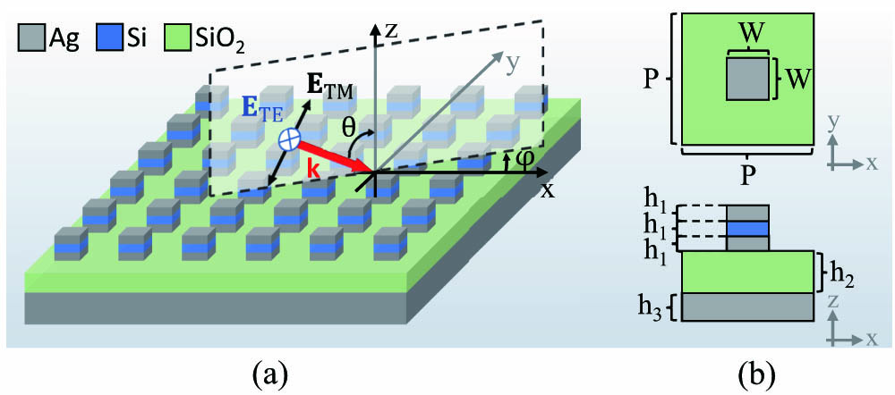
Fig. 1. Schematic of the plasmonic metasurface. (a) The plasmonic metasurface consists of periodic arrays of Ag–Si–Ag nanoblocks, a SiO2 spacer, and a bottom Ag layer. In the incident plane, θ represents the elevation angle of incidence between the wave vector k and the z axis. The azimuth angle between the incident plane and the x axis is denoted by φ. (b) Top and front views of a unit cell of the metasurface.
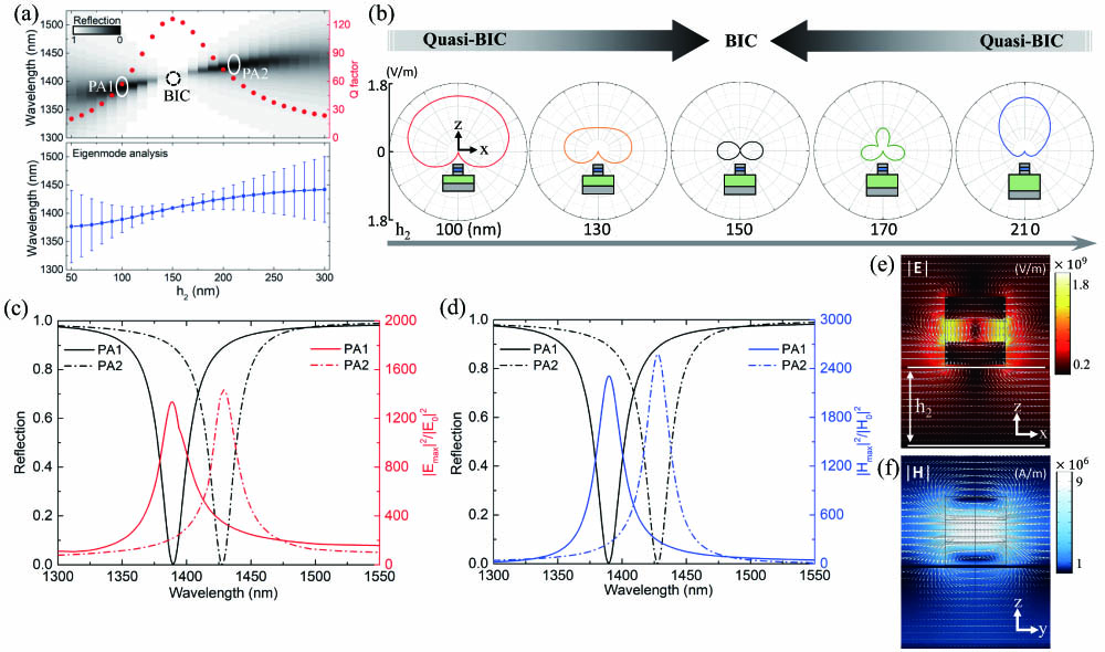
Fig. 2. Simulation results of normal incidence. (a) Reflection spectra and eigenmode Q-factors (red dots) of the plasmonic metasurface versus the spacer thickness in the case of normal incidence by an x-polarized plane wave (upper half). Eigenmode spectra and the FWHM extracted from the reflection spectra are shown by blue dots and error bars, respectively (lower half). (b) The far-field radiation patterns of a unit cell show the evolution from quasi-BICs to the BIC when changing h2. (c), (d) Electric and magnetic field enhancement of the two PAs (PA1 at h2=100 nm, PA2 at h2=210 nm), respectively. (e), (f) Electric and magnetic field distributions of PA2, respectively, when the wavelength is 1428 nm.
Fig. 3. Simulation results of oblique incidence. (a) Schematic of obliquely incident plane waves in the case of zero azimuth angle (φ=0°); (b), (c) the reflection spectra and Q-factors versus the elevation angle (θ) of incidence under the illumination of TM and TE plane waves in the x-z incident plane when h2=100 nm and h2=210 nm, respectively. The white dashed curves represent contours with a reflection of 0.1. (d) Schematic representation of an x-polarized plane wave propagating through an objective onto the metasurface; (e), (f) the reflection against different θ and φ of incidence in the cases of h2=100 nm at the wavelength of 1390 nm and h2=210 nm at the wavelength of 1428 nm, respectively, where the yellow contours represent a reflection of 0.1. Polarization distributions in different incident planes of the focused light corresponding to (d) are illustrated in (g), (h), and (i).
Fig. 4. Average reflection of plasmonic metasurfaces. (a) Schematic of multiangle incidence. The incident light contains TM and TE plane waves with equal intensity. Two azimuth angles of φ=0° (blue region) and 45° (red region) are considered. The elevation angle θ varies from 0° to 30° in steps of 2°. (b) The average reflection spectra in the cases of h2=100 nm and h2=210 nm.
Fig. 5. Band structures and Q-factors of the plasmonic metasurface when h2=210 nm. M1 and M2 represent the eigenmodes in which the polarization direction of the magnetic field is mainly perpendicular and parallel to the reciprocal lattice vector kT, respectively. (a) Magnetic field profiles of M1 and M2. (b), (c) Eigenwavelengths of M1 and M2, respectively, the black contours represent λr=1423 nm. (d), (e) Equivalent elevation angles of M1 and M2, respectively, the yellow dashed contours represent θ=28°. (f), (g) Q-factors of M1 and M2, respectively.
Fig. 6. Simulation settings. Floquet periodic boundary conditions were applied in the x and y directions. Two PMLs were added in the z direction at the top and bottom of the physical domain.
Fig. 7. Multipole decomposition of the plasmonic metasurface. The radiated power versus wavelength contributed by ED, MD, TD, EQ, and MQ when an x-polarized plane wave illuminates on the metasurface from the normal direction. (a) h2=100 nm; (b) h2=210 nm.
Fig. 8. Reflection spectra of oblique incidence when φ=45° in the cases of (a) h2=100 nm and (b) h2=210 nm. The white dashed curves represent contours with a reflection of 0.1.
Fig. 9. Influence of fabrication deviations when h2=210 nm. (a) Schematic of deviations. The first case is that corners are deformed into rounded corners, where R represents the radius of rounded corners. The second case is a pyramid-like deformation, where the side length of the top surface Wt is smaller than that of the bottom surface W. (b) Average reflection spectra in the case of rounded corners; (c) average reflection spectra in the case of pyramid-like deformation.