Abstract
664 GHz sub harmonic mixer for ice cloud detection was designed and fabricated, based on 0.5 μm “T” anode GaAs SBD membrane integrated process with thickness of 5 μm. Parasitic parameters of “T” anode design were analyzed and membrane process was developed to improve high frequency performance. The mixer was characterized in 664 GHz receiver setup. Double side band conversion loss of the mixer was 9.9 dB at 664 GHz room temperature.Introduction
As an important application area of terahertz technology,monitoring ice clouds from airplane or satellite with terahertz heterodyne receivers can provide data for atmosphere water cycle research and precise weather report. It has been supported by several airplane or satellite payload programs such as NASA’s CoSSIR[1],ESA’s ISMAR[2] and ICI[3]. 664GHz is one of the ice particle sensitive channels included by above programs. GaAs SBD mixer is usually considered as a compact,low noise technique for 664GHz airborne heterodyne receiver[4].
As a basic element of terahertz mixer,GaAs SBD has been developed for decades from the early dot-matrix whisker-contacted style to planar type [5]. With the commercial success,structural improvement reports of GaAs SBD become rare,while research focus has shifted to the new materials such as GaN SBD [6] and InP SBD [7]. However,GaAs SBD maintain its status as high cutoff frequency,low noise,low cost device ready to meet higher and higher frequency demand of varies terahertz application. Therefor a GaAs SBD is still needed to be evolved both at device structure and integrated process constantly.
For working frequency at 664GHz,traditional circuits on 25~50μm GaAs or quartz substrate are not suitable because substrate mode effect and transition loss become severer[8]. To alleviate substrate effects in high terahertz circuit,GaAs membrane integrated process has been developed and demonstrated to sustain SBD circuit of frequency up to 2.7 THz [9].
In this paper a 664 GHz sub-harmonic mixer based on 5μm membrane GaAs SBD process was presented. “T” shape anode contact was designed and analyzed to indicate a new way to improve cutoff frequency ft. The membrane mixer chip was packaged in a waveguide module for measurement. Double side band(DSB)conversion loss of 9.9 dB at 664 GHz was achieved.
1 Device design and fabrication
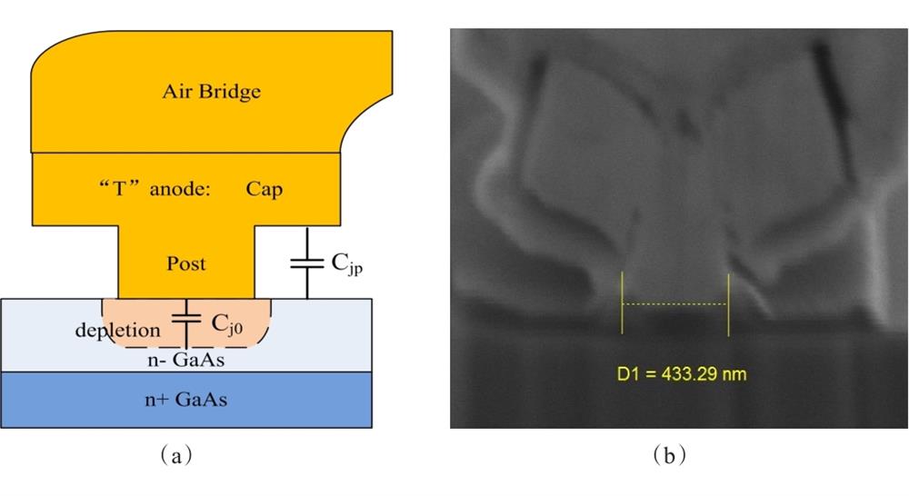
Analogous to HEMT T gate [10],a circular “T” shape anode contact metal of GaAs SBD was designed. Compared with contact metal deposited in SiO2 anode well [11],“T” anode could provide a smaller junction parallel capacitance Cjp(in some paper denoted as part of Cfp)while scaling down anode diameter into sub micron anode area,and maintaining a large contact area with air bridge metal. Cjp of “T” anode mainly originates from metal “cap”(see Fig. 1(a)). Therefore,increasing “post” metal height could directly reduce Cjp.

Figure 1.“T” shape anode of GaAs SBD: (a) schematic picture with Cjp and Cj0; (b) SEM picture of 0.5 μm anode metal section.
| Layer function | Material | Doping | Thickness |
|---|
| Schottky contact | GaAs | n-,1e17cm-3 | 100nm |
| Ohmic contact | GaAs | n+,7e18cm-3 | 1μm |
| Membrane | GaAs | nid | 5μm |
| Etch-stop | AlGaAs | nid | 50nm |
| Substrate | GaAs | S.I. | / |
Table 1. Epitaxy layer structure of GaAs SBD membrane circuit
In order to have a higher performance at 664 GHz,epitaxy material was optimized(as shown in Table 1). Additional undoped GaAs layer and an etch-stop AlGaAs layer was inserted beneath n+GaAs layer,worked as the membrane substrate instead of the original GaAs substrate.
To investigate the relationship between diode performance and anode dimension,“T” anode GaAs SBD with different anode diameter from 0.5 μm(shown in Fig. 1(b))to 2.1 μm were fabricated. Rs was extracted through IV curves. Cj0 and Cjp as a total junction capacitance was extracted through S parameters. In order to distinguish Cjp from Cj0,C-V measurement were carried out on large anode(diameter range from 50 μm to 200 μm)SBD devices on the same wafer. While Cjp could be neglected compared with Cj0 of these large diodes,the extracted capacitance per anode area was 2.4fF/μm2,which could be used to calculated the intrinsic Cj0 of small anode diodes.
Extracted Rs,Cj0 and Cfp were compared in Fig. 2(a). While scaling down anode area,1/Rs deviated from linear with anode area because of complicated current distribution in n-/n+ GaAs beneath anode. Particularly,in the anode area region below 1μm2,the slope of 1/Rs shown a flattening tread,which helped increase intrinsic cutoff frequency ft calculating with only Rs and Cj0,as shown in Fig. 2(b). It indicated a smaller anode area would have a higher ft. For the 0.5μm diameter diode,intrinsic ft reached 10.5 THz. However,Cjp didn’t show a linear relationship with anode area,which stopped ft’ calculated with Rs and Cj0+Cjp increasing while reducing anode area. The highest ft’ reached 7.7 THz. Therefore,in odder to improve ft’ by scaling down anode area below 1 μm2,efforts should be paid on decreasing Cjp. For “T” anode design,increasing “post” metal height would be a direct way.
Figure 2.Characteristics of “T” shape anode GaAs SBD with different anode size: (a)Cj0, Cjp and 1/Rs versus anode area; (b)ft versus anode diameter.
2 Mixer design and fabrication
As depicted in fig. 3(a),to halve LO frequency require,sub harmonic mixer structure was adopted based on our 5 μm GaAs membrane process. Compared with hybrid integrated quartz circuit,monolithic integrated membrane circuit is virtually immune from alignment error and substrate mode effect. Anti parallel SBD structure was used to suppress odd order harmonic component and increase the sub harmonic component. Suspended micro strip probes were designed to connect RF/LO waveguide with CPW main circuit. Edge of CPW’s ground metal and DC ground connect component was fabricated as suspended beamlead in chip process,and welded on the metal cavity. In order to sustain membrane chip’s mechanical strength,several breaks along CPW’s ground line were inserted to release stress between metal and GaAs membrane which originated from chip process.
0.5 μm anode diameter diode was chosen for mixer design instead of 1.1 μm diode which has a better ft’ because when designing the mixer circuit,estimation of different SBD had not finished. 0.5 μm was expected to have a better performance when Cjp was under-evaluation.
Figure 3.GaAs membrane sub harmonic mixer design: (a) 3D design diagram; (b) microscope picture of the finished mixer.
Fabrication process started with cathode contact deposition and annealing. Then “T” shape anode contact was vaporized,followed by air bridge electroplating. After mesa etching,CPW and beamlead metal was electroplated on the membrane layer surface. When finished the front side processes,the wafer substrate was mechanically thinned,polished and etched completely,leaving back side of the membrane layer exposed. Finally membrane process were finished by removing gap area between chips through backside lithography and etching. The sub harmonic mixer of “T” anode GaAs SBD membrane process was finished and welded in the metal housing as shown in Fig. 3(b).
3 Receiver module demonstration
A 664 GHz receiver was assembled based on our membrane sub harmonic mixer,as shown in Fig. 4(a). 24x multiplier chain module was connected to the LO waveguide,provided 3 mW LO power. IF port was connected with a low noise amplifier(LNA). To estimate double side band conversion loss,measurement setup was established as shown in Fig. 4(b). A black body radiation source was used as cold and hot noise source. Frequency synthesizer provided fundamental frequency for the multiplier chain. Spectrum analyzer was used to monitor IF output.
Y factor measurement[12] was conducted under 77 K and 290 K. IF frequency was fixed at 3GHz. Subtracting LNA and antenna’s noise figure,double side band(DSB)conversion loss of the mixer was attained. As shown in Fig. 5,DSB conversion loss was less than 11dB in 654~675 GHz range,and less than 14 dB in 646~677 GHz range. Optimum value was 9.9 dB attained at 664 GHz.
Figure 4.Pictures of 664GHz receiver (a) and measurement setup (b)
Figure 5.Measured and simulated DSB conversion loss of the membrane mixer
The simulated DSB conversion loss was also depicted in Fig. 5,showed 4~5 dB lower than measured data,indicating potentials of “T” anode GaAs SBD membrane process has not been fully developed.
4 Conclusion
Sub micron “T” anode GaAs SBD and 664GHz sub harmonic membrane mixer were reported. Performance of “T” anode GaAs SBD with different anode area was investigated to further improve ft in sub micron anode region. 664 GHz sub harmonic mixer based on 0.5 μm GaAs SBD with 5μm GaAs membrane chip was designed and fabricated. DSB conversion loss of 9.9 dB at 664GHz was achieved.
References
[1] Evans , K. Franklin et al. Ice Cloud Retrievals and Analysis with the Compact Scanning Submillimeter Imaging Radiometer and the Cloud Radar System during CRYSTAL FACE. Journal of Applied Meteorology, 44, 839-859(2005).
[2] S Fox, C Lee, I Rule et al. ISMAR: A new Submillimeter Airborne Radiometer(2014).
[3] V Kangas, S D'Addio, U Klein et al. Ice cloud imager instrument for MetOp Second Generation(2014).
[4] E , Defer , C et al. Development of precipitation retrievals at millimeter and sub-millimeter wavelengths for geostationary satellites. Journal of Geophysical Research Atmospheres(2008).
[5] F Sizov. THz radiation sensors. Opto-Electronics Review, 18, 10-36(2010).
[6] Y Sun, X Kang, Y Zheng et al. Review of the Recent Progress on GaN-Based Vertical Power Schottky Barrier Diodes (SBDs). Electronics, 8, 575(2019).
[7] H Ito, I Tadao. InP/InGaAs Fermi-level managed barrier diode for broadband and low-noise terahertz-wave detection. Japanese Journal of Applied Physics(2016).
[8] J Treuttel, L Gatilova, A Maestrini et al. A 520–620-GHz Schottky Receiver Front-End for Planetary Science and Remote Sensing With 1070 K–1500 K DSB Noise Temperature at Room Temperature. IEEE Transactions on Terahertz Science and Technology, 1-8(2015).
[9] Chattopadhyay , G. Technology. Capabilities, and Performance of Low Power Terahertz Sources. IEEE Transactions on Terahertz Science & Technology, 1, 33-53(2011).
[10] B O Lim, M K Lee, T J Baek et al. 50-nm T-Gate InAlAs/InGaAs Metamorphic HEMTs With Low Noise and High fT Characteristics. IEEE Electron Device Letters, 28, 546-548(2007).
[11] S M Marazita, W L Bishop, J L Hesler et al. Integrated GaAs Schottky mixers by spin-on-dielectric wafer bonding. IEEE Transactions on Electron Devices, 47, 1152-1157(2000).
[12] D M Pozar. Microwave Engineering, 4th Edition(2005).