Abstract
Metasurfaces have become a new photonic structure for providing potential applications to develop integrated devices with small thickness, because they can introduce an abrupt phase change by arrays of scatterers. To be applied more widely, active metasurface devices are highly desired. Here, a tunable terahertz meta-lens whose focal length is able to be electrically tuned by is demonstrated experimentally. The lens consists of a metallic metasurface and a monolayer graphene. Due to the dependence of the abrupt phase change of the metasurface on the graphene chemical potential, which can be modulated using an applied gate voltage, the focal length is changed from 10.46 to 12.24 mm when the gate voltage increases from 0 to 2.0 V. Experimental results are in good agreement with the theoretical hypothesis. This type of electrically controlled meta-lens could widen the application of terahertz technology.1. INTRODUCTION
In the past decade, terahertz (THz) technology has aroused enormous interest in the science and application communities due to its great application potentials from information and communications to security, quality monitoring of agricultural products, and biological and medical sciences [1,2]. Although promising steps have been taken, the great challenge of lack of miniaturization and system integration still remains due to the large and bulky scale of the optical components in this frequency region [3]. Metasurfaces, composed of arrays of metallic or dielectric micro/nano scatterers, may be a possible solution and have been studied intensively [4–7]. Unlike conventional optical devices realizing phase modulation by optical path accumulation, the metasurface devices introduce an abrupt modulation of light wavefront in two-dimensional (2D) space, and thus ultrathin optical components are able to be realized. For example, achromatic meta-lenses based on dielectric resonators have been proposed, which may replace traditional multi-lens combinations [8,9]. At THz frequencies, many functional metasurface structures with deep subwavelength thickness have also been proposed for wave deflection, focusing, imaging, and polarization selection [10–13].
In order to achieve wavefront control, reconfigurable imaging, and dynamical holography, active metasurfaces are highly desired. However, a metallic or dielectric-only metasurface lacks tunability once the structure is complete, limiting the application of these kinds of 2D modulators. To address this problem, many materials have been proposed recently that enable metasurfaces to be actively tunable, such as phase-change materials [14,15], oxide-semiconductor field-effect transistors [16], and stretchable substrates [17]. Unfortunately, all of these devices work in the visible or near-infrared regime. In addition, these tuning mechanisms, which are based on force, heat, or magnetic fields, suffer a slow tuning speed. Graphene, a typical 2D material consisting of a single atomic layer of hexagonal carbon lattice [18], has become an outstanding photonics material nowadays [19]. Besides the ultra-thin thickness, graphene also has the intriguing merit that its optical properties can be changed using chemical doping or electrostatic gating with a high speed of (MHz) [20–22]. Furthermore, this tuning mechanism is also valid at THz frequencies due to the intra-band electron-photon scattering processes [23]. Consequently, active THz metasurfaces can be developed using graphene. In 2011, Ju et al. proposed a graphene grating for tuning the intensity of a transmitted THz wave [24]. Then several tunable metamaterial structures assisted by the graphene were theoretically or experimentally proposed for wave intensity modulation and surface plasmon polariton modulation [25–28]. In 2015, tunable hybrid metal–graphene plasmons and a graphene-based THz spatial light modulator were reported [29,30]. A systematic study of tunable phase modulation in the THz regime by metallic metasurfaces combined with gate-tuned graphene was presented both theoretically and experimentally [31]. In 2018, a hybrid active metamaterial structure combined with metallic split-ring resonators and graphene was reported, which was able to realize both large intensity and phase tuning [32].
In this paper, an electrically tunable THz lens using a hybrid structure of a metallic metasurface and a monolayer graphene is described. The interaction of the THz wave with the structure can be modulated by the graphene chemical potential, which is tuned using an applied gate voltage, resulting in the phase of the transmitted THz wave to be actively controlled. The focus is shifted by 1.78 mm () when the gate voltage changes from 0 to 2.0 V. Experimental results are in good agreement with the theoretical hypothesis.
Sign up for Photonics Research TOC. Get the latest issue of Photonics Research delivered right to you!Sign up now
2. DESIGN AND FABRICATION
The schematic structure of the tunable THz meta-lens is depicted in Fig. 1(a). The lens is composed of a high-resistance silicon substrate and a gold film etched with rectangular aperture antennas. Each antenna has different length and rotation angle , as shown in the scanning electron microscope (SEM) photograph (detected by SHIMADZU SSX-550) of a unit cell of the apertures. The gold metasurface in the plane is covered by a graphene layer to achieve the active tuning of transmitted THz. The monolayer graphene is grown by the chemical vapor deposition (CVD) method [33,34] and characterized using the Raman scattering spectrum (detected by RENISHAW RM2000), plotted in Fig. 1(b). The G peak and 2D peak () are clearly observed [35,36]. A gate voltage is applied using two electrodes attached to the metal and graphene separately to tune the graphene chemical potential . The incident THz wave is left-handed circularly polarized (LCP), propagating along the axis.
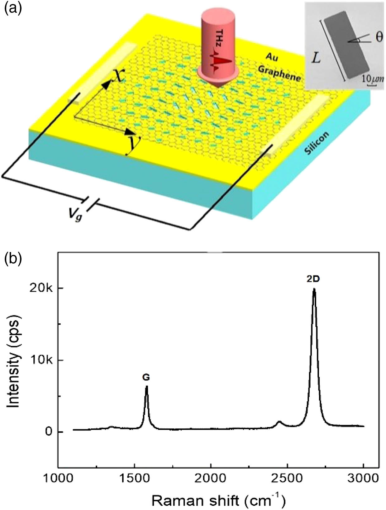
Figure 1.(a) Schematic of the active THz meta-lens. The lens consists of a high-resistance silicon substrate, an Au metasurface of rectangular aperture antennas with different lengths and rotations, and a monolayer graphene. The incident THz wave is left-handed circularly polarized. The inset shows an SEM photograph of a unit cell of the apertures. (b) Raman spectrum of the monolayer graphene on the top of the Au metasurface.
In order to design a focus-tunable THz lens, the phase control of each metasurface unit must fulfill two conditions. First, the phase distribution of the units needs to ensure that all wavelets are in phase at the focal point, i.e., the phase is determined by [6] where is the designed focal length, and is the incident wavelength. Second, when the graphene chemical potential varies consistently, the phase change needs to be different for different apertures. For example, if the phase is increased by the graphene chemical potential, and the corresponding phase change is increased monotonically from the middle to the edge of the lens, the focal length will decrease, otherwise it will increase. Therefore, the Pancharatnam–Berry (PB) phase-based metasurface structure [37] is employed. When an LCP wave transmits through a rectangular aperture with a rotation angle , an abrupt phase change of will occur for the transmitted right-handed circularly polarized (RCP) wave, and thus condition 1 is satisfied by the rotation of the apertures. Condition 2 can be addressed by introducing different lengths of the apertures, because the resonance of THz waves from apertures of different sizes has diverse responses in changing the graphene chemical potential [21]. Figure 2 shows the simulated abrupt phase and transmission of transmitted RCP THz wave through one rectangular aperture, dependent on the aperture length, under different graphene chemicals. The sweep simulations are conducted using the finite-difference time-domain (FDTD) method with a commercial software (Lumerical FDTD Solutions). In the simulations, the incident THz frequency is 0.75 THz, and the incident LCP THz wave is radiated by two orthogonal linearly polarized plane waves with a phase difference of . The detected RCP wave is calculated by , where and are the electric field component in the and direction, respectively. The aperture width is fixed as 20 μm. It is found in Fig. 2(a) that when is increased, the abrupt phase is decreased, and the phase change increases with the aperture length. For example, the phase reduction corresponding to increased from 0.1 to 0.5 eV, is when . However, it increases to when . The transmission is increased with , due to the enlarged aperture when is increased, which can be seen in Fig. 2(b). In addition, the transmission is decreased with . The reason could be that the conductivity of graphene is increased with the chemical potential, enhancing the screening effect of THz waves [37]. Furthermore, when the graphene effective permittivity is changed by , the resonant frequency of the aperture antenna would have a small shift, causing the transmission to be lower [21].

Figure 2.Dependence of transmitted RCP THz wave on the aperture length and graphene chemical potential. The aperture width is fixed as 20 μm. (a) Phase change of RCP THz wave as a function of , when changes from 0.1 to 0.5 eV. (b) Transmission of RCP THz wave as a function of , when changes from 0.1 to 0.5 eV.
Following a design method based on this principle [37], the active THz lens in Fig. 1(a) is then designed. The radius of the lens is 2.0 mm, with 540 cells. The period of the aperture array is 150 μm in both the and directions. All the aperture widths are 20 μm. The incident THz frequency is 0.75 THz. The focal length is designed to increase from 7.0 to 9.0 mm. The corresponding phase distribution of the two focal lengths and on the axis, calculated by Eq. (1), are shown in Fig. 3(a). The phase difference is depicted as the red dotted line, which gives the corresponding phase modulation depth of the units. It is found that varies from 0 to . Therefore, the aperture length in the range of [50,150] μm satisfies the phase difference requirement in Fig. 3(a), when increases from 0.1 to 0.5 eV. Then all the aperture lengths are determined using the results in Figs. 2(a) and 3(a). In our design, because the transmission variation dependent on is relatively small, we only consider the phase modulation. The corresponding and of the 540 apertures of the designed lens are shown in Figs. 3(b) and 3(c), respectively.
Figure 3.Design of the meta-lens. The focal length is designed to increase from 7.0 to 9.0 mm, when changes from 0.1 to 0.5 eV. (a) The corresponding phase distributions (blue lines) of focal lengths are 7.0 and 9.0 mm, respectively, and the phase difference (red line) between them is shown. Phase distribution as a function of the aperture length dependent on the graphene chemical potential. (b) Length and (c) rotation angle distributions of the apertures of the proposed tunable lens.
The development process of the sample is depicted in Fig. 4(a). A high-resistance silicon substrate with size of and thickness of 500 μm is prepared first. Then a layer of S1813 photoresist is produced on the substrate using a spin coating process with a speed of 2000 r/min. After that, an ultraviolet (UV) lithography system (Karl Süss MA6) is used to generate the metasurface pattern of photoresist under a Cr plated quartz mask. In the third step, an electron beam evaporation coating is used to add a 10 nm Cr layer and 100 mm Au layer onto the top of the sample, with a deposition rate of 0.5 Å/s and vacuum pressure of . A lift-off process is then performed to achieve an Au metasurface, and the CVD-produced monolayer graphene is transferred onto the top of the metasurface structure. In the end, two contact electrodes Cr (5 nm)/Au (60 nm) are adhered to the Au and graphene layers, separately, using evaporation coating. An SEM photo of the fabricated sample is shown in Fig. 4(b). The gate voltage is applied by a Keithley 4200 semiconductor characterization system.
Figure 4.(a) Fabrication process of the electrically tunable THz meta-lens. (b) SEM micrograph of the fabricated device.
3. RESULTS AND DISCUSSION
The electrical tuning mechanism of the active meta-lens is characterized using a THz focal plane imaging system, which is able to achieve both intensity and phase information of a circularly polarized THz wave by detecting two orthogonal linearly polarized THz radiations [13]. Each image of the transmitted RCP THz wave needs to be measured twice (vertical and horizontal linearly polarized waves), which is time-consuming and may cause an unstable applied gate voltage across a long period of detection. Therefore, only the intensity and phase distributions of an image plane at for and are recorded. The corresponding measured transmitted RCP THz wave intensity and phase distributions are depicted as Figs. 5(a)–5(d). A bright spot is observed on the image plane. It is also observed that both the intensity and phase distributions change when the gate voltage increases, indicating that it is able to modulate the wavefront of a THz wave electrically. The far-field distribution of the THz wave is then calculated using the Huygens–Fresnel principle [38] in which where is the electric field component of the transmitted RCP wave. , , and are the coordinates of the imaging plane. is the wave vector in the vacuum. is the distance between the far-field observation point and a point on the imaging plane. In Figs. 5(e) and 5(f), the field distributions of the transmitted RCP THz wave on the plane for and are shown, respectively. It can be seen that the focusing effect can be observed clearly in both pictures, which demonstrates the lens function of the proposed device. More importantly, the focal tuning is achieved by the gate voltage. The focal length is 10.46 mm when no voltage is applied, and changed to 12.24 mm when is 2.0 V. The focus is changed by 1.78 mm (). This tuning range is very close to the designed value (2.0 mm), although the experimental focal lengths are larger than the designed ones (from 7.0 to 9.0 mm). For ease of comparison, the field intensity is normalized to the maximum value in Fig. 5(e). It is found that the transmitted field intensity is decreased slightly after the gate voltage is applied. This could be due to the static voltage increasing the conductivity of graphene, enhancing the screening effect of THz waves [37]. By the method proposed in Ref. [21], we estimate the modulation speed of the device to be .
Figure 5.Experimental results of the tunable meta-lens. (a) and (b) Measured transmitted RCP THz wave intensity (normalized) and phase (rad) distributions of the imaging plane with a distance of 2.0 mm behind the meta-lens when , respectively. (c) and (d) Measured intensity (normalized) and phase (rad) distributions of the imaging plane when , respectively. (e) and (f) Calculated far-field intensity distribution of RCP THz wave based on the measured intensity and phase of the imaging plane when and , respectively. The frequency of the incident THz wave is 0.75 THz.
In order to look into the tuning mechanism of the lens, we then conduct FDTD simulation studies. The graphene chemical potentials corresponding to the applied gate voltages of 0 V and 2.0 V, respectively, need to be determined first. The position of the charge-neutral Dirac point of the graphene is found by measuring the electrical resistance of the graphene on the sample. The result is shown in Fig. 6(a). It is found that the Dirac point corresponding to the maximum resistance appeared when . When a gate voltage is applied, the carrier density of graphene can be calculated as [39] where is the elementary charge, and and are the permittivity and thickness of the dielectric between graphene and Au. In this device, the coupling effect of the graphene and metallic structure is significantly decreased with the distance between the graphene and Au. Therefore, in order to enhance the modulation of the graphene, the graphene layer is attached directly to the metasurface. It is assumed there is a 1 nm thick air layer between the graphene and Au. On the other hand, the relationship between the carrier density and chemical potential can be expressed as [40] where is the reduced Planck constant, and is the Fermi velocity. Therefore, according to Eqs. (4) and (5), the graphene chemical potentials corresponding to and are estimated to be and , respectively, which are close to the designed chemical potentials. FDTD simulations of the device are then performed under these two chemical potentials. The results are shown in Figs. 6(b) and 6(c). It is found that the simulated focal lengths are 11.95 mm and 13.76 mm for the two chemical potentials, and the focal tuning range is 1.81 mm, which is in good agreement with the experimental results. That the experimental focuses deviate from the designed ones may be caused by the fabrication errors in the aperture lengths.
Figure 6.Simulation results of the active lens. (a) Gate-dependent electrical resistance of the graphene on the metasurface. (b) and (c) FDTD simulations of far-field intensity distribution of RCP THz wave when and , respectively.
4. CONCLUSIONS
In conclusion, an active THz meta-lens assisted by graphene based on phase modulation is proposed. The lens consists of a metallic metasurface structure based on a PB phase and a monolayer graphene. Due to the coupling effect of the THz wave and the hybrid graphene-metal structure, the phase of transmitted THz wave is able to be tuned electrically using an applied gate voltage. The meta-lens is fabricated and characterized. Both simulation and experimental results demonstrate that the focus is able to be shifted by . It is anticipated that the proposed structure may open up an avenue to achieve tunable THz devices using graphene.
Acknowledgment
Acknowledgment. The authors thank Mr. Zhiyuan Du for his help with the experimental work.
References
[1] M. Tonouchi. Cutting-edge terahertz technology. Nat. Photonics, 1, 97-105(2007).
[2] T. Nagatsuma, G. Ducournau, C. C. Renaud. Advances in terahertz communications accelerated by photonics. Nat. Photonics, 10, 371-379(2016).
[3] X. C. Zhang, A. Shkurinov, Y. Zhang. Extreme terahertz science. Nat. Photonics, 11, 16-18(2017).
[4] N. Yu, P. Genevet, M. A. Kats, F. Aieta, J.-P. Tetienne, F. Capasso, Z. Gaburro. Light propagation with phase discontinuities reflection and refraction. Science, 334, 333-337(2011).
[5] A. V. Kildishev, A. Boltasseva, V. M. Shalaev. Planar photonics with metasurfaces. Science, 339, 1232009(2013).
[6] N. Yu, F. Capasso. Flat optics with designer metasurfaces. Nat. Mater., 13, 139-150(2014).
[7] P. Genevet, F. Capasso, F. Aieta, M. Khorasaninejad, R. Devlin. Recent advances in planar optics: from plasmonic to dielectric metasurfaces. Optica, 4, 139-152(2017).
[8] M. Khorasaninejad, F. Aieta, P. Kanhaiya, M. A. Kats, P. Genevet, D. Rousso, F. Capasso. Achromatic metasurface lens at telecommunication wavelengths. Nano Lett., 15, 5358-5362(2015).
[9] W. T. Chen, A. Y. Zhu, V. Sanjeev, M. Khorasaninejad, Z. Shi, E. Lee, F. Capasso. A broadband achromatic metalens for focusing and imaging in the visible. Nat. Nanotechnol., 13, 220-226(2018).
[10] X. Zhang, Z. Tian, W. Yue, J. Gu, S. Zhang, J. Han, W. Zhang. Broadband terahertz wave deflection based on C-shape complex metamaterials with phase discontinuities. Adv. Mater., 25, 4567-4572(2013).
[11] D. Hu, X. Wang, S. Feng, J. Ye, W. Sun. Ultrathin terahertz planar elements. Adv. Opt. Mater., 1, 186-191(2013).
[12] Q. Yang, J. Gu, D. Wang, X. Zhang, Z. Tian, C. Ouyang, R. Singh, J. Han, W. Zhang. Efficient flat metasurface lens for terahertz imaging. Opt. Express, 22, 25931-25939(2014).
[13] S. Wang, X. Wang, Q. Kan, J. Ye, S. Feng, W. Sun, P. Han, S. Qu, Y. Zhang. Spin-selected focusing and imaging based on metasurface lens. Opt. Express, 23, 26434-26441(2015).
[14] X. Yin, T. Steinle, L. Huang, T. Taubner, M. Wuttig, T. Zentgraf, H. Giessen. Beam switching and bifocal zoom lensing using active plasmonic metasurfaces. Light Sci. Appl., 6, e17016(2017).
[15] C. H. Chu, M. L. Tseng, J. Chen, P. C. Wu, Y. H. Chen, H. C. Wang, T. Y. Chen, W. T. Hsieh, H. J. Wu, G. Sun, D. P. Tsai. Active dielectric metasurface based on phase-change medium. Laser Photon. Rev., 10, 986-994(2016).
[16] Y. W. Huang, H. W. H. Lee, R. Sokhoyan, R. A. Pala, K. Thyagarajan, S. Han, D. P. Tsai, H. A. Atwater. Gate-tunable conducting oxide metasurfaces. Nano Lett., 16, 5319-5325(2016).
[17] H. S. Ee, R. Agarwal. Tunable metasurface and flat optical zoom lens on a stretchable substrate. Nano Lett., 16, 2818-2823(2016).
[18] A. K. Geim, K. S. Novoselov. The rise of graphene. Nat. Mater., 6, 183-191(2007).
[19] A. N. Grigorenko, M. Polini, K. S. Novoselov. Graphene plasmonics. Nat. Photonics, 6, 749-758(2012).
[20] M. C. Sherrott, P. W. C. Hon, K. T. Fountaine, J. C. Garcia, S. M. Ponti, V. W. Brar, L. A. Sweatlock, H. A. Atwater. Experimental demonstration of >230° phase modulation in gate-tunable graphene-gold reconfigurable mid-infrared metasurfaces. Nano Lett., 17, 3027-3034(2017).
[21] Y. Yao, M. A. Kats, P. Genevet, N. Yu, Y. Song, J. Kong, F. Capasso. Broad electrical tuning of graphene-loaded plasmonic antennas. Nano Lett., 13, 1257-1264(2013).
[22] P. Q. Liu, I. J. Luxmoore, S. A. Mikhailov, N. A. Savostianova, F. Valmorra, J. Faist, G. R. Nash. Highly tunable hybrid metamaterials employing split-ring resonators strongly coupled to graphene surface plasmons. Nat. Commun., 6, 8969(2015).
[23] L. A. Falkovsky, S. S. Pershoguba. Optical far-infrared properties of a graphene monolayer and multilayer. Phys. Rev. B, 76, 153410(2007).
[24] L. Ju, B. Geng, J. Horng, C. Girit, M. Martin, Z. Hao, H. A. Bechtel, X. Liang, A. Zettl, Y. R. Shen, F. Wang. Graphene plasmonics for tunable terahertz metamaterials. Nat. Nanotechnol., 6, 630-634(2011).
[25] B. Vasić, M. M. Jakovljević, G. Isić, R. Gajić. Tunable metamaterials based on split ring resonators and doped graphene. Appl. Phys. Lett., 103, 011102(2013).
[26] W. Zhu, I. D. Rukhlenko, M. Premaratne. Graphene metamaterial for optical reflection modulation. Appl. Phys. Lett., 102, 241914(2013).
[27] S. Cakmakyapan, L. Sahin, F. Pierini, W. Strupinski, E. Ozbay. Resonance broadening and tuning of split ring resonators by top-gated epitaxial graphene on SiC substrate. Appl. Phys. Lett., 103, 181116(2013).
[28] C. Zeng, X. Liu, G. Wang. Electrically tunable graphene plasmonic quasicrystal metasurfaces for transformation optics. Sci. Rep., 4, 5763(2014).
[29] M. M. Jadidi, A. B. Sushkov, R. L. Myers-Ward, A. K. Boyd, K. M. Daniels, D. K. Gaskill, M. S. Fuhrer, H. D. Drew, T. E. Murphy. Tunable terahertz hybrid metal-graphene plasmons. Nano Lett., 15, 7099-7104(2015).
[30] N. Kakenov, T. Takan, V. A. Ozkan, O. Balcı, E. O. Polat, H. Altan, C. Kocabas. Graphene-enabled electrically controlled terahertz spatial light modulators. Opt. Lett., 40, 1984-1987(2015).
[31] Z. Miao, Q. Wu, X. Li, Q. He, K. Ding, Z. An, Y. Zhang, L. Zhou. Widely tunable terahertz phase modulation with gate-controlled graphene metasurfaces. Phys. Rev. X, 5, 041027(2015).
[32] O. Balci, N. Kakenov, E. Karademir, S. Balci, S. Cakmakyapan, E. O. Polat, H. Caglayan, E. Ozbay, C. Kocabas. Electrically switchable metadevices via graphene. Sci. Adv., 4, eaao1749(2018).
[33] K. S. Kim, Y. Zhao, H. Jang, S. Y. Lee, J. M. Kim, K. S. Kim, J. H. Ahn, P. Kim, J. Y. Choi, B. H. Hong. Large-scale pattern growth of graphene films for stretchable transparent electrodes. Nature, 457, 706-710(2009).
[34] X. Li, W. Cai, J. An, S. Kim, J. Nah, D. Yang, R. Piner, A. Velamakanni, I. Jung, E. Tutuc, S. K. Banerjee, L. Colombo, R. S. Ruoff. Large area synthesis of high quality and uniform graphene films on copper foils. Science, 324, 1312-1314(2009).
[35] A. C. Ferrari, J. C. Meyer, V. Scardaci, C. Casiraghi, M. Lazzeri, F. Mauri, S. Piscanec, D. Jiang, K. S. Novoselov, S. Roth, A. K. Geim. Raman spectrum of graphene and graphene layers. Phys. Rev. Lett., 97, 187401(2006).
[36] W. Liu, B. Hu, Z. Du, Z. Wang, X. Zhou, J. Liu, Y. Wang. Enhanced electric tuning of Raman scattering in monolayer graphene by gold nanorods. Plasmonics, 13, 275-280(2018).
[37] Z. Huang, B. Hu, W. Liu, J. Liu, Y. Wang. Dynamical tuning of terahertz meta-lens assisted by graphene. J. Opt. Soc. Am. B, 34, 1848-1854(2017).
[38] M. Born, E. Wolf. Principals of Optics, 561(1999).
[39] V. E. Dorgan, M. H. Bae, E. Pop. Mobility and saturation velocity in graphene on SiO2. Appl. Phys. Lett., 97, 082112(2010).
[40] L. A. Falkovsky. Optical properties of graphene. J. Phys. Conf. Ser., 129, 012004(2008).


