
Daigao Chen, Hongguang Zhang, Min Liu, Xiao Hu, Yuguang Zhang, Dingyi Wu, Peiqi Zhou, Siyao Chang, Lei Wang, Xi Xiao, "67 GHz light-trapping-structure germanium photodetector supporting 240 Gb/s PAM-4 transmission," Photonics Res. 10, 2165 (2022)
- Photonics Research
- Vol. 10, Issue 9, 2165 (2022)
Abstract
1. INTRODUCTION
With the rapid growth of worldwide data transmission requirements, high-speed, low-cost, and small-sized optical interconnection has made great progress in the last decades. Owing to the compatibility with commercial complementary metal–oxide–semiconductor (CMOS) processes, silicon photonics (SiP) has the advantages of large-scale monolithic integration, small footprint, and low cost [1–3], which enables it to be one of the most promising technologies for optical interconnection. Various high-performance SiP devices, including passive and active devices, have been reported in several works [4–11], which also indicates that SiP chips occupy an important place in the high-speed optical communication industry.
A photodetector (PD) is one of the crucial devices of SiP technology. Due to the indirect bandgap, silicon has low absorption efficiency at C- and O-bands. Thus, it usually grows germanium (Ge) to fabricate PD in a SiP circuit [12–14]. There are two basal structures of Ge waveguide PDs: lateral PIN [9,10,15–22] and vertical PIN [11,21–32]. All of these PDs have been reported with high opto-electrical (OE) bandwidths. For lateral PIN PD, IHP developed a 265 GHz lateral Ge PD fabricated by a special process with highly accurate alignment of lithography and precise adjustment of critical dimensions [9]. In 2016, a 67 GHz lateral PIN Ge PD was fabricated by IMEC’s SiP platform [10]. Based on this PD, a 100 Gb/s on–off keying (OOK) return-to-zero (RZ) signal was detected. For a vertical PIN PD, over 60 GHz bandwidth is reported in Refs. [11,23,24]. In Ref. [11], a Ge PD with a lateral silicon nitride input waveguide is demonstrated to support 150 Gb/s four-level pulse amplitude modulation (PAM-4) signal detection with 1 mA photocurrent.
Generally, the shape of the Ge absorption region is rectangular for both lateral and vertical PIN PDs. Optical signal is input from one side of the rectangle, and unabsorbed signal is output from the opposite side. The absorption coefficient of Ge decreases at longer wavelengths and rolls off rapidly around 1600 nm [33,34]. To improve responsivity, especially at longer wavelengths, generally it needs to lengthen the rectangular Ge absorption region. However, increasing the length means increasing parasitic parameters, i.e., capacitance [30], which will degrade the bandwidth. That is to say, there is a trade-off between the responsivity and bandwidth of a Ge PD with a rectangular absorption region. Some works employ reflection structures in the device to increase the responsivity and shorten the length [31,32].
In this work, we propose a novel light-trapping-structure Ge waveguide PD to realize high OE bandwidth and high responsivity simultaneously. At
2. DEVICE DESIGN
There are two typical light-trapping structures: photonic crystal and circular. For photonic crystal structure, such as a grating, Ge is difficult to fabricate. In this work, we choose the circular light-trapping structure. The schematic of the proposed vertical-PIN Ge PD is shown in Fig. 1. It is fabricated on a commercial standard silicon-on-insulator (SOI) wafer with a 3 μm thick box layer and a 220 nm thick top silicon layer. The input Si waveguide is a rib waveguide, and the etching depth of the Si layer is about 130 nm; 500 nm thick Ge is selectively grown on the unetched Si area. The top of Ge is N-doped, and the silicon under Ge is P-doped.
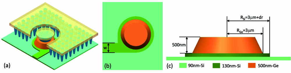
Figure 1.Schematic of the light-trapping-structure Ge PD: (a) 3D view, (b) top view, and (c) side view along the incident direction; (b) and (c) hide all metal layers. Doping is not shown.
As shown in Fig. 1, the Ge absorption area and unetched Si under Ge are circular. The silicon input waveguide is tangent to the silicon circle. Based on the boundary condition for an electromagnetic field, when the incident angle is larger than the critical angle, the input light will be totally reflected. Thus, if the radius of the circle is large enough, and the incident angle is appropriate, the light will be trapped in the light-trapping region and propagate along the edge of the circle. Then the Ge absorption region can be reused during light propagation, and the carriers will be generated until the trapped light is completely absorbed. As a result, with the same volume, the circular structure can increase the responsivity of the PD. The improvement in responsivity is more effective at longer wavelengths, since the absorption coefficient at longer wavelengths is lower than that at shorter wavelengths. Due to the responsivity improvement of the light-trapping structure, the size of the absorption region can be small. The parasitic parameters, such as the capacitance of the PN junction, can also be small. Thus, compared with rectangular PDs, which use long absorption regions to increase responsivity, the proposed PD can get a better RF bandwidth without sacrificing responsivity.
The proposed PD is modeled and simulated by Ansys Lumerical FDTD Solutions. In the simulation, the absorption coefficient of Ge is set to
![]()
Figure 2.Field distributions at different wavelengths in the proposed PD. (a)–(d) Distributions in silicon layer and (e)–(h) distributions in germanium layer.
As shown in Figs. 2(e)–2(h), input light propagates along the edge of the Ge mesa, while in the center of the circle, the field distribution is weak. Thus, if the metal contact is placed in the center of the Ge circle, the absorption of metal will be minimum.
Then, we add the metal contact in the model and simulate the responsivity again with the optimized parameters. We detect the electric field distribution in the Ge mesa with a 3D monitor, and then calculate the absorbance of Ge using the detected field distribution. According to Eq. (1), we can calculate the responsivity
![]()
Figure 3.Calculated responsivity of the circular Ge PD.
The simulated responsivity shows ripples especially at longer wavelengths. Ripples come from the resonance in the Ge mesa. Because the absorption of Ge decreases as wavelength increases, the resonance becomes stronger at longer wavelengths, which induces stronger ripples at longer wavelengths.
3. EXPERIMENTAL RESULTS
The PD is fabricated by a commercial SiP platform. Figure 4 shows an optical micrograph of the fabricated PD. Received optical signal is coupled into the PD chip by a grating coupler (GC). A linear taper used as a spot size converter connects the single mode waveguide and the input waveguide of the PD. The PD has three electrical pads arranged as ground-signal-ground (GSG) mode. The performance of the PD is tested by static measurement, small-signal RF measurement, and optical signal transmission measurement.
![]()
Figure 4.Optical micrograph of the fabricated circular Ge PD.
A. Static Measurement
Static measurements include dark current and responsivity measurements. We used a Santec tunable laser as the light source, and a Kethiley source meter to supply the bias voltage. The light source was turned off when measuring the dark current, and turned on when measuring the responsivity. The measured dark current versus bias voltage (
![]()
Figure 5.(a) Dark current versus voltage and (b) normalized responsivity at different wavelengths.
In Fig. 5(a), the proposed PD shows low dark currents, which is about 2.9 and 6.4 nA at
B. Small-Signal RF Measurement
The OE bandwidth of the proposed circular Ge PD is obtained by small-signal RF measurement. A 67 GHz Keysight light wave component analyzer (LCA) is employed with a built-in laser and modulator. A 67 GHz GSG probe is used to connect the pad of the PD. The reverse bias voltage is supplied by a Keithley source meter through a bias tee. Optical signal generated from the LCA is detected by the PD, and the converted RF signal is output through the bias tee. In the measurement, the bandwidth influence from RF cables and probes is calibrated. The normalized frequency responses with different bias voltage are shown in Fig. 6. At 0 V, the 3 dB bandwidth is about 26 GHz. With bias voltage increasing, the 3 dB bandwidth increases rapidly, and can reach 55 and 67 GHz at
![]()
Figure 6.Normalized frequency response of the proposed Ge PD.
There are two major factors that can affect the OE bandwidth of the typical PIN PD: the transit time of carriers and capacitance–resistance (RC) constant. The 3 dB bandwidth can be calculated by
For our light-trapping Ge PD, the photon lifetime may also affect the bandwidth. As shown in Fig. 2, received light propagates along the edge of the circular absorption area. Because the absorption coefficient at longer wavelengths is weak, the light circulates several times until it is completely absorbed. A long propagation time means a long photon lifetime. However, for the 3 μm radius circle, even if the light propagates 10 circles, the propagation time is about 2.5 ps (group index of Ge is assumed to be four), which corresponds to a 400 GHz bandwidth, much larger than the measured 67 GHz bandwidth. Thus, the influence of propagation time can be neglected.
According to the above analyses, we can qualitatively explain the bandwidth variation of the proposed PD at different voltages. At 0 V, due to the weak electric field in Ge, the velocities of carriers are low and
Table 1 gives a performance comparison of bandwidth, responsivity, and dark current between our PD and other works. Benefiting from the light-trapping circle and compressed absorption area, the proposed PD can relax the trade-off between bandwidth and responsivity to a certain extent.
Performance Comparison between Proposed PD and Other Works
| Reference | Structure of Ge | 3 dB Bandwidth | Responsivity | Dark Current | Dark Current | |
|---|---|---|---|---|---|---|
| [ | Rectangle ( | 265 at 2 V | 0.3 at 1550 nm | |||
| [ | Rectangle ( | 67 at 1 V | 0.74 at 1550 nm | 3.6 at 2 V | ||
| [ | Rectangle | 67 at 2 V | 0.9 at 1550 nm | – | 90 at 1 V | |
| [ | Rectangle ( | 42 at 4 V | 1 at 1550 nm | 18 at 1 V | 60 | |
| [ | Rectangle ( | 31 at 2 V | 0.89 at 1550 nm | 169 at 2 V | 51 | |
| [ | Rectangle ( | 40 at 1 V | 0.7 at 1550 nm | 1.16 at 1 V | ||
| [ | Rectangle ( | 45 at 1 V | 0.8 at 1500 nm (TM mode) | 3 at 1 V | ||
| Our previous work | Rectangle ( | 35 at 3 V | 0.85 at 1550 nm | 20 at 2 V | 25 | |
| This work | Circular ( | 67 at 2 V | 1.05 at 1550 nm 0.78 at 1580 nm | 6.4 at 2 V | 23 | |
Data calculated using the referenced paper.
C. High-Speed Transmission Measurement
The performance of the proposed PD in a high-speed optical transmission system is verified by measuring the BER and eye diagram of PAM-4 signal. The experiment setup is shown in Fig. 7(a). In our experiment, various baud rates of PAM-4 signal are generated by an arbitrary waveform generator (AWG) whose sampling rate is 120 GS/s (Keysight M8194A). The output amplitude of AWG is
![]()
Figure 7.(a) Experiment setup of high-speed PAM-4 signal transmission system and (b) BTB eye diagram of 80, 90, 100, and 105 GBaud PAM-4 signals.
In our experiment, offline DSP is utilized on both Tx and Rx sides to jointly optimize the performance of the transmission system. In Tx DSP, a pseudo random bit sequence (PRBS) PAM-4 signal is generated with a word length of
Figure 7(b) shows a BTB eye diagram of the PAM-4 signal with different baud rates. In the measurement, a
The transmission BERs of the PAM-4 signal with different bit rates and transmission distances are measured and demonstrated in Fig. 8(a). The highest bit rate for BTB is 240 Gb/s with a BER of
![]()
Figure 8.(a) BER versus different bit rates with BTB, 1 km, and 2 km transmissions; (b) BTB BER of 200 Gb/s PAM-4 versus different optical power.
To analyze the receiver sensitivity of 100 GBaud/s PAM-4 signal transmission, we tested the BTB BER with various received optical powers. The result is shown in Fig. 8(b). We also used the SD-FEC threshold as the criteria, and the receiver sensitivity was
4. CONCLUSION
We proposed and demonstrated a novel light-trapping-structure vertical Ge PD. In our scheme, circular Ge with 3 μm radius is designed to constrain the optical signal in the absorption area. Benefiting from the light-trapping circle, the trade-off between bandwidth and responsivity can be relaxed. With
References
[1] R. Soref. The past, present, and future of silicon photonics. IEEE J. Sel. Top. Quantum Electron., 12, 1678-1687(2006).
[2] N. Izhaky, M. T. Morse, S. Koehl, O. Cohen, D. Rubin, A. Barkai, G. Sarid, R. Cohen, M. J. Paniccia. Development of CMOS-compatible integrated silicon photonics devices. IEEE J. Sel. Top. Quantum Electron., 12, 1688-1698(2006).
[3] X. Chen, M. M. Milosevic, S. Stanković, S. Reynolds, T. D. Bucio, K. Li, D. J. Thomson, F. Gardes, G. T. Reed. The emergence of silicon photonics as a flexible technology platform. Proc. IEEE, 106, 2101-2116(2018).
[4] A. Y. Piggott, J. Lu, K. G. Lagoudakis, J. Petykiewicz, T. M. Babinec, J. Vučković. Inverse design and demonstration of a compact and broadband on-chip wavelength demultiplexer. Nat. Photonics, 9, 374-377(2015).
[5] B. Shen, P. Wang, R. Polson, R. Menon. An integratednanophotonics polarization beamsplitter with 2.4 × 2.4 μm2 footprint. Nat. Photonics, 9, 378-382(2015).
[6] M. Li, L. Wang, X. Li, X. Xiao, S. Yu. Silicon intensity Mach–Zehnder modulator for single lane 100 Gb/s applications. Photon. Res., 6, 109-116(2018).
[7] M. Sakib, P. Liao, C. Ma, R. Kumar, D. Huang, G.-L. Su, X. Wu, S. Fathololoumi, H. Rong. A high-speed micro-ring modulator for next generation energy-efficient optical networks beyond 100 Gbaud. Conference on Lasers and Electro-Optics, SF1C.3(2021).
[8] Y. Zhang, H. Zhang, M. Li, P. Feng, L. Wang, X. Xiao, S. Yu. 200 Gbit/s optical PAM4 modulation based on silicon microring modulator. European Conference on Optical Communication, Th3A-1(2020).
[9] S. Lischke, A. Peczek, J. S. Morgan, K. Sun, D. Steckler, Y. Yamamoto, F. Korndörfer, C. Mai, S. Marschmeyer, M. Fraschke, A. Krüger, A. Beling, L. Zimmermann. Ultra-fast germanium photodiode with 3-dB bandwidth of 265 GHz. Nat. Photonics, 15, 925-931(2021).
[10] H. Chen, P. Verheyen, P. De Heyn, G. Lepage, J. De Coster, S. Balakrishnan, P. Absil, W. Yao, L. Shen, G. Roelkens, J. Van Campenhout. −1 V bias 67 GHz bandwidth Si-contacted germanium waveguide p-i-n photodetector for optical links at 56 Gbps and beyond. Opt. Express, 24, 4622-4631(2016).
[11] X. Hu, D. Wu, H. Zhang, W. Li, D. Chen, L. Wang, X. Xiao, S. Yu. High-speed and high-power germanium photodetector with a lateral silicon nitride waveguide. Photon. Res., 9, 749-756(2021).
[12] Y. Ishikawa, K. Wada. Germanium for silicon photonics. Thin Solid Films, 518, S83-S87(2010).
[13] J. Wang, S. Lee. Ge-photodetectors for Si-based optoelectronic integration. Sensors, 11, 696-718(2011).
[14] W. N. Ye, Y. Xiong. Review of silicon photonics: history and recent advances. J. Mod. Opt., 60, 1299-1320(2013).
[15] G. Dehlinger, S. J. Koester, J. D. Schaub, J. O. Chu, Q. C. Ouyang, A. Grill. High-speed germanium-on-SOI lateral PIN photodiodes. IEEE Photon. Technol. Lett., 16, 2547-2549(2004).
[16] J. Kang, S. Takagi, M. Takenaka. Ge photodetector monolithically integrated with amorphous Si waveguide on wafer bonded Ge-on-insulator substrate. Opt. Express, 26, 30546-30555(2018).
[17] D. Benedikovic, L. Virot, G. Aubin, J. M. Hartmann, F. Amar, X. Le Roux, C. Alonso-Ramos, E. Cassan, D. Marris-Morini, P. Crozat, F. Boeuf, J. M. Fedeli, C. Kopp, B. Szelag, L. Vivien. 40 Gbps heterostructure germanium avalanche photo receiver on a silicon chip. Optica, 7, 775-783(2020).
[18] D. Benedikovic, L. Virot, G. Aubin, F. Amar, B. Szelag, B. Karakus, J.-M. Hartmann, C. Alonso-Ramos, X. Le Roux, P. Crozat, E. Cassan, D. Marris-Morini, C. Baudot, F. Boeuf, J.-M. Fédéli, C. Kopp, L. Vivien. 25 Gbps low-voltage hetero-structured silicon-germanium waveguide pin photodetectors for monolithic on-chip nanophotonic architectures. Photon. Res., 7, 437-444(2019).
[19] L. Virot, D. Benedikovic, B. Szelag, C. Alonso-Ramos, B. Karakus, J.-M. Hartmann, X. Le Roux, P. Crozat, E. Cassan, D. MarrisMorini, Ch. Baudot, F. Boeuf, J.-M. Fédéli, C. Kopp, L. Vivien. Integrated waveguide PIN photodiodes exploiting lateral Si/Ge/Si heterojunction. Opt. Express, 25, 19487-19496(2017).
[20] X. Hu, D. Wu, H. Zhang, W. Li, D. Chen, L. Wang, X. Xiao, S. Yu. High-speed lateral PIN germanium photodetector with 4-directional light input. Opt. Express, 28, 38343-38354(2020).
[21] K.-W. Ang, T.-Y. Liow, M.-B. Yu, Q. Fang, J. Song, G.-Q. Lo, D.-L. Kwong. Low thermal budget monolithic integration of evanescent-coupled Ge-on-SOI photodetector on Si CMOS platform. IEEE J. Sel. Top. Quantum Electron., 16, 106-113(2010).
[22] T.-Y. Liow, K.-W. Ang, Q. Fang, J.-F. Song, Y.-Z. Xiong, M.-B. Yu, G.-Q. Lo, D.-L. Kwong. Silicon modulators and germanium photodetectors on SOI: monolithic integration, compatibility, and performance optimization. IEEE J. Sel. Top. Quantum Electron., 16, 307-315(2010).
[23] F. Boeuf, A. Fincato, L. Maggi, J. F. Carpentier, P. Le Maitre, M. Shaw, S. Cremer, N. Vulliet, C. Baudot, S. Monfray, S. Jan, C. Deglise, J. R. Manouvrier, C. Durand, A. Simbula, D. Goguet, P. Bar, D. Ristoiu, F. Leverd, L. Babaud, A. Daverio, M. Binda, A. Bazzotti, A. Canciamilla, L. Ramini, M. Traldi, P. Gambini. A silicon photonics technology for 400-Gbit/s applications. IEEE International Electron Devices Meeting (IEDM), 33.1.1-33.1.4(2020).
[24] D. Zhu, J. Zheng, Y. Qamar, O. Martynov, F. Rezaie, E. Preisler. A high performance Ge PIN photodiode compatible with high volume silicon photonics production processes. IEEE 15th International Conference on Group IV Photonics (GFP), 1-2(2018).
[25] L. Vivien, J. Osmond, J.-M. Fédéli, D. Marris-Morini, P. Crozat, J.-F. Damlencourt, E. Cassan, Y. Lecunff, S. Laval. 42 GHz p.i.n germanium photodetector integrated in a silicon-on-insulator waveguide. Opt. Express, 17, 6252-6257(2009).
[26] T. Yin, R. Cohen, M. M. Morse, G. Sarid, Y. Chetrit, D. Rubin, M. J. Paniccia. 31 GHz Ge n-i-p waveguide photodetectors on silicon-on-insulator substrate. Opt. Express, 15, 13965-13971(2007).
[27] M. M. P. Fard, G. Cowan, O. Liboiron-Ladouceur. Responsivity optimization of a high-speed germanium-on-silicon photodetector. Opt. Express, 24, 27738-27752(2016).
[28] D. Ahn, C. Hong, J. Liu, W. Giziewicz, M. Beals, L. C. Kimerling, J. Michel. High performance, waveguide integrated Ge photodetectors. Opt. Express, 15, 3916-3921(2007).
[29] M. J. Byrd, E. Timurdogan, Z. Su, C. V. Poulton, N. M. Fahrenkopf, G. Leake, D. D. Coolbaugh, M. R. Watts. Mode-evolution-based coupler for high saturation power Ge-on-Si photodetectors. Opt. Lett., 42, 851-854(2017).
[30] C. T. DeRose, D. C. Trotter, W. A. Zortman, A. L. Starbuck, M. Fisher, M. R. Watts, P. S. Davids. Ultra compact 45 GHz CMOS compatible germanium waveguide photodiode with low dark current. Opt. Express, 19, 24897-24904(2011).
[31] J. Cui, Z. Zhou. High-performance Ge-on-Si photodetector with optimized DBR location. Opt. Lett., 42, 5141-5144(2017).
[32] C. Lin, D. Huang, T. Shih, H. Kuo, S. Chang. Increasing responsivity-bandwidth margin of germanium waveguide photodetector with simple corner reflector. Opt. Express, 29, 10364-10373(2021).
[33] M. Rouvière, M. Halbwax, J.-L. Cercus, E. Cassan, L. Vivien, D. Pascal, M. Heitzmann, J.-M. Hartmann, S. Laval. Integration of germanium waveguide photodetectors for intrachip optical interconnects. Opt. Eng., 44, 75402-75406(2005).
[34] L. M. Nguyen, R. Kuroyanagi, T. Tsuchizawa, Y. Ishikawa, K. Yamada, K. Wada. Stress tuning of the fundamental absorption edge of pure germanium waveguides. Opt. Express, 23, 18487-18492(2015).


Set citation alerts for the article
Please enter your email address

© Copyright 2018-2021 | Chinese Laser Press. All Rights Reserved 沪ICP备15018463号-20