M. Y. Shubar, H. L. Saadon, Saeed J. Abbas, "Nonlinear optical switching and all-figures of merit in Bi2S3-xSex/PMMA nanocomposite films investigated by Z scan under visible CW laser," Chin. Opt. Lett. 18, 011902 (2020)
Copy Citation Text
Bi2S3-xSex/poly(methyl methacrylate) (PMMA) nanocomposite films were prepared using microwave assisted synthesis with different compositions of x. Crystal structure, surface morphology, and optical properties were investigated to characterize the prepared nanocomposite films. The crystallinity and optical band gap of the prepared Bi2S3-xSex/PMMA were affected by x. The prepared samples showed a blue shift in the absorption edge. The laser power dependent nonlinear refraction and absorption of Bi2S3-xSex/PMMA nanocomposite films were investigated by using the Z-scan technique. The optical nonlinearity of the nanocomposite films exhibited switchover from negative nonlinear refraction to positive nonlinear refraction to negative nonlinear refraction effects, and from saturable absorption to reverse saturable absorption to saturable absorption with an increase and decrease in the composition. An interesting all-optical figure of merit was reported to assess the nanocomposite films for a practical device. It was calculated that the device all-figures of merit were based on the nonlinear response, which is important for the all-optical switching device. The results demonstrate that the optimized all-optical figures of merit can be achieved by adjusting the composition and input laser power, which can be used for the design of different all-photonic devices, and the results of nonlinear switching behavior can open new possibilities for using the nanocomposite films in laser Q-switching and mode-locking.
The basic limitations on the nonlinear optical (NLO) response have contributed to understanding the light-material interactions[1]. To date, the emphasis in the creation of NLO materials has improved NLO properties[2,3]. Investigation of nonlinear response is significant due to its wide range of applications in all-photonics applications. Suitable NLO materials, which exhibit nonlinear absorption (NLA) and nonlinear refraction (NLR), are required for optoelectronic device fabrication. The nonlinear process that involves saturable absorption (SA), reverse SA (RSA), positive NLR (PNLR), negative NLR (NNLR) behaviors depends on the incident wavelength, incident power, and material concentration[4–9]. Nanomaterials are very interesting because of their unique physical and chemical properties and their potential applications in many optical fields. The NLO effects of semiconductor nanocrystals have attracted huge attention in the last several years due to the large NLO responses[10,11].
The material requirements for all-optical photonic devices that can be understood in terms of all-optical figures of merit (FOMs) are the physics limitations in the sense that it is deep-seated in the physics of the optical nonlinearities of the NLO materials[12]. These devices will develop to light controlling with light[13]. In this stage, the all-optical technologies are based on all-optical switching, which is only possible in NLO materials[14,15]. Therefore, all-optical switching is a key technology for all-photonic technology.
Nanocomposite materials containing semiconductors in a polymer matrix can be introduced as new NLO materials. There is still a need for a material with very low losses and large NLO parameters. Among all materials, the bismuth sulfide () semiconductor can be very useful in all-photonic devices, such as the all-optical switching or all-optical devices and all-optical limiting.
Sign up for Chinese Optics Letters TOC. Get the latest issue of Chinese Optics Letters delivered right to you!Sign up now
In this Letter, we prepared (methyl methacrylate) (PMMA) nanocomposite films at different compositions of and investigated their NLO properties. The nonlinear Kerr coefficient , NLA coefficient , and their all-optical FOMs were obtained by the Z-scan technique using CW neodymium-doped yttrium aluminum garnet (Nd:YAG) laser radiation at a wavelength of 532 nm.
All of the following chemicals are used as received without any further treatments: bismuth chloride (reagent grade, 98%), thiourea (Alfa, 99%), ethylene glycol (EG, Riedel-de Haen, 99%), telluride (Fluka, 99%), chloroform (Scharlau, synthesis grade stabilized with ethanol), sodium selenite (CDH analytical reagent, 99%), and PMMA powder (reagent grade, 97%).
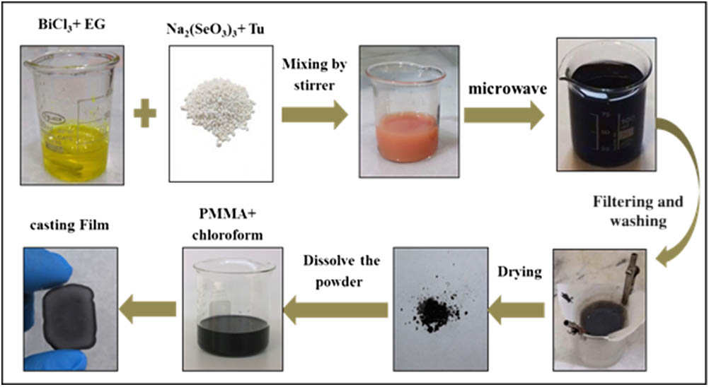
Bismuth chalcogenides (S, Se) are prepared by microwave assisted synthesis. The representative scheme of the method is illustrated in Fig. 1. Firstly, the source of bismuth () is dissolved carefully in 12.5 mL of EG with the help of magnetic stirring. Secondly, the source of chalcogen anion (S or Se to S ratio) is added to the solution of the bismuth with a conducted continuous stirring. Here, we have studied the effect of change of the mole fraction of Se with respect to S on the properties of the ternary compound (, , 0.2, 0.4, and 1). Finally, the mixed solution is exposed to microwave radiation. To avoid the excess pressure generated by heat, we used open reactor with on/off times of the microwave power equal to 10 s/20 s for 2 min. The microwave power is provided from a commercial microwave oven with a radiated power 720 W. The black precipitate is filtered by a filter paper and washed several times by distilled water and ethanol to remove any unreacted materials. Then, the filtrate is left in a petri dish at 60°C for 2 h to dry.
Figure 1.Schematic steps of the sample preparation process.
The lack of the bismuth semiconductor compounds to solution processing is to make it a thin film for practical application. We composed it with polymer PMMA, which has good optical and mechanical properties, as well as good solubility in many popular solvents. Finally, nanocomposite films of are prepared, where , 0.2, 0.4, and 1 (we wanted to point out that throughout this article, refers to the molar ratio between sodium selenite to the thiourea in the solution, which means the ratio of Se to S). We thoroughly mix the same amount of the semiconductor and PMMA polymer (0.02 g of each) in 5 mL chloroform under vigorous magnetic stirring for 1 h. The films are deposited on glass substrates and left to dry naturally at the room temperature. The obtained films have a uniform surface, and their thickness is approximately in the range of . The crystalline structure of the prepared samples was investigated using X-ray diffraction (XRD) (PANalytical X’PertPRO with α; 1.5406 A radiation). The morphology was observed by a scanning electron microscope (SEM, NOVA NAAOSEM 450) with an energy dispersive X-ray (EDX) unit attached to it for inspection of the elemental composition, while optical absorption was investigated by a UV-visible (UV-vis) 1800 spectrophotometer within the wavelength range of 300–800 nm.
A schematic of the experimental setup of the Z-scan technique is shown in Fig. 2. The Z-scan technique is used to measure the intensity dependence of the NLA coefficient and nonlinear refractive index (or nonlinear Kerr coefficient) of materials. In this technique, one measures the intensity of a tightly focused Gaussian laser beam as a function of position of the sample under investigation, which is scanned across the focal plane. Here, the input power of the laser beam is varied by using a natural density filter (NDF). A CW Nd:YAG laser at the 532 nm wavelength is used as an excitation source. After passing through a spatial filter, the laser beam is focused onto the sample by a convex lens L3 of 50 mm focal length, which leads to a Rayleigh length of equal to 2.8 mm and a radius of the beam waist of . Afterward, a beam-splitter (BS) divides the beam into two parts. The first beam passes through detector 1 after passing through a convex lens (L5), while the other one is focused by a convex lens (L4). Two detectors connected to a data acquisition controller (DAQ) are used to record the signal of the laser beam, and the transmitted intensity is monitored by a computer (DAQ and computer not shown in the figure).
Figure 2.Experimental setup of Z-scan technique. NDF, natural density filter; L, lens; SF, spatial filter; S, sample; A, aperture.
The XRD patterns of at different compositions, , 0.2, 0.4, and 1, are shown in Fig. 3. All of the diffraction peaks are labeled and can be indexed to an orthorhombic structure. All patterns (i.e., for all Se to S ratios) exhibit the same crystal structure as the binary (i.e., ). The lattice constants are Å, Å, and ÅÅ; these values are well in agreement with the standard [Joint Committee on Powder Diffraction Standards (JCPDS) No. 170320][16]. All of the main peaks are the same in each pattern, but there is a small shift due to the difference of the atomic radius of Se and S atoms[17], while replacing the S with Se makes no change in crystal structures. Here, a systematic shift of the most intense XRD peaks for the (122) plane was observed[16], and there were high crystallization peaks for the (122) plane and low crystallization in the (131) and (130) planes. The XRD peak intensity increased when the Se:S ratio reaches 0.3, indicating the enhanced crystallinity of prepared nanocomposites. At , there was a decrease in the crystallinity, as shown in Fig. 3(b); similar results have been reported of other nanocomposite materials[18,19].
Figure 3.(a) X-ray diffraction patterns of nanocomposite films at different compositions, , 0.2, 0.4, and 1. (b) The peak intensity as a function of composition.
The surface morphology (SEM images) of is shown in Fig. 4 at different compositions of . The SEM images show that there are two kinds of nanostructures. One is a nanowire, and the other is a nanosheet. It can be revealed that the prepared samples have good surface morphology and quality. As shown in the figure, the nanowires have an average length of 1640 nm and a width of 47.3 nm. The ternary sample has an average length equal to 241.4 nm with a width of 56.72 nm. The formation of nanowires at and 0.4 that have a more directional growth in a certain axis is confirmed with the XRD results, and that ratio has the higher crystallinity, as shown in Fig. 3.
Figure 4.SEM images of nanocomposite films at four different compositions, , 0.2, 0.4, and 1.
The EDX spectra (Fig. 5) confirmed the semiconductor formation. All of the elements that form the are present in the EDX spectra. In addition to the constitution elements, there is a peak in carbon, which is attributed to the grid that is used in the measurement, and a peak of oxygen comes from the aqueous solution during the preparation or processing.
Figure 5.EDX spectrum of nanocomposite films for composition (a) and (b) .
Figure 6 shows the optical absorption spectra of nanocomposite films at different compositions of . All of the samples have a broad absorption character over the entire visible region; this property is required in many applications, including light absorbing dependence. According to Tauc’s law[20], the optical band gap can be determined by the equation where is the absorption coefficient, is the optical band gap, is a constant, and is a parameter that depends on the type of electronic transition, which is responsible for the absorption ( for direct transition). The inset in Fig. 6 shows plot of versus photon energy (). The values of the energy gap of nanocomposite films are 2.07, 2.17, and 2.35 eV for , 0.2, and 0.4, respectively. The optical band gap of bulk is 1.3 eV (absorption edge of 946.15 nm)[21]. We observed that the prepared nanocomposite films exhibited a blue shift in the absorption edge for these ratios compared to the absorption edge of bulk . When the Se:S ratio is equal to 1, the optical band gap decreases to the value 1.88 eV. This lowering in the optical band gap can be attributed to the becoming richer with Se than S. Because of that, the optical band gap of bismuth selenide is less than from the , which leads to this lowering. This case is similar to the other materials[22].
Figure 6.Optical absorption spectra of nanocomposite films with different compositions of 0, 0.2, 0.4, and 1. The inset is the plot of as a function of .
The NLO response of the prepared samples was investigated using the Z-scan technique. Figure 7 shows the NLO response of nanocomposite films with different compositions, , 0.2, 0.4, and 1. The normalized transmission of nanocomposite samples was measured as a function of the sample position (z) for Z-scan results at varying input powers. The Z-scan data give us information about the NLO refractive index and NLA parameters. It can be observed that the variation of these parameters with increasing composition leads to the changing of the sign of the nonlinear refractive index from negative to positive [Fig. 7(I)] and NLA from SA to RSA and then to SA with a change in Se concentration [Fig. 7(II)].
Figure 7.(I) Closed-aperture and (II) open-aperture Z-scan results at different input powers of the nanocomposite films with different compositions: (a) 0, (b) 0.2, (c) 0.4, and (d) 1. The solid lines are theoretical fitting.
It is interesting in Fig. 7 that the behaviors of the NLR and NLA change in the prepared nanocomposite films at different sample compositions from 0 up to 1. In the nonlinear refractive regime, the nanocomposite films with compositions of 0 and 0.4 exhibit a negative refractive index, while the nanocomposite films at 0.2 and 1 composition display a positive refractive index. Indeed, the results show that the nanocomposite films change over in the behaviors related to the response of the input laser beam. That means the NNLR is changed to PNLR and vice versa when increases with the increase of composition, as shown in Table 1. The change in the sign of the nonlinear refractive index behavior can be interpreted by the fact that as the Se concentration ratio of the excited electrons increases, the NLR effect in self-focusing is enhanced, which is similar to the case of the other materials[23–25].
Input Power (mW)
n2×10−10(m2/W)
β×10−4(m/W)
W
T
Composition, x
Composition, x
Composition, x
Composition, x
0
0.2
0.4
1.0
0
0.2
0.4
1.0
0
0.2
0.4
1.0
0
0.2
0.4
1.0
5
−1.774
8.1
−8.7
11.14
−4
12.6
20.5
−5.7
0.93
0.7
3.57
4.5
1.19
0.81
1.2
0.3
7
−1.75
6.1
−6.6
10.5
−3
9.19
16.3
−6.18
0.92
0.5
2.7
4.33
0.75
0.79
1.32
0.31
10
−1.47
6.97
−5
7.9
−2
7
10
−4.65
0.77
0.6
2
3.2
0.72
0.53
1.1
0.31
13
−1.4
5.79
−3.45
6.98
−1
5.6
7.9
−5.42
0.74
0.5
1.4
2.8
0.36
0.51
1.2
0.41
Table 1. Nonlinear Optical Coefficients and Figures of Merit of Bi2S3−xSex/PMMA Nanocomposite Films with Four Different Compositions of 0, 0.2, 0.4, and 1 at 532 nm Laser Excitation
In the NLA regime, the nanocomposite films correspond to the compositions of 0 and 1, and the SA gets gradually reinforced. Also, the nanocomposite films prepared with compositions of 0.2 and 0.4 were found to be switched to RSA. That means the SA turns to RSA when increases with the increase of composition. Then, increasing the composition up to 1, the film was switched to SA again with decrease, as shown in Table 1. The change in the NLA behaviors can be related to the film absorbing the laser beam and could probably generate enough carriers to fill band states up to and including those of the optical transition. Then, the interplay of the absorption band leads to bleach. This phenomenon is similar to the case of the other materials[23–25].
From the above results in Fig. 7, it can be seen that the NLR and NLA responses show a changeover in the sign of the optical nonlinearity. This can also be attributed generally to the polymer matrix or the dispersing agent used, and maybe the polymer leads to a dispersion in the prepared nanocomposite films. In addition, shapes of nanostructures have an important effect on the NLO behaviors, as shown in Fig. 4. In addition, the efficient control of NLA response can lead to the applications in the mode-locking laser and in the protection from laser damage to eyes.
The physical mechanism of the NLR in NLO material can be electronic, molecular, and thermal in the natural effect[26,27]. Under CW laser, the nanocomposite films are expected to be due to the thermal effect. This could be confirmed by the fact that the closed aperture Z-scan curves satisfy the condition of electronic refractive nonlinearity. In order to apply the theory of Z-scan[27], the distance separation between the transmittance at the peak–valley in the direction is to be .
Using the value of and the Z-scan curves in Fig. 7, the value of can be calculated and found to be more than 1.7 times the Rayleigh length , since the origin of the optical nonlinear refractive index is thermal nonlinearity in nature.
The values of nonlinear refractive index can be calculated by the equation[27]where is the linear transmittance of the aperture given by , where is the radius of the laser spot before the aperture, is the radius of the aperture, and is the phase shift given by the relationship[27]where is the peak–valley transmittance difference from the closed aperture Z-scan curve, is the effective thickness of the sample given by , is the wave vector, is the intensity of the laser beam at the focus, and is the linear adsorption. The normalized transmittance in the case of closed aperture Z-scan is[27]where .
In addition, the physical mechanism of the NLA can be due to a change in absorption with increasing or decreasing intensity. That can be SA, which leads to a decrease in the absorption of light in the material, and RSA, which leads to an increase in absorption of light in the material[28,29]. RSA and SA can be caused by two-photon absorption (TPA), free carrier absorption (FCA), and nonlinear scattering. When the energy band gap , the TPA is the dominant mechanism. In the present work, the results are attributed to SA and RSA in the origin of the nanocomposite films. Hence, the TPA is insignificant. The NLA can be given by[27]where is the normalized transmittance. The normalized transmission is given by[27]where , and is an integer.
In practice, for an NLO material to be good in such a device, it must have not only as large a nonlinear refractive index and small an NLA coefficient as possible, but also satisfactory “all-optical FOMs”[30]. Therefore, the all-optical FOMs are used to evaluate the quality of the NLO material for all-photonic devices. Thus, two all-optical FOMs are defined as[31]and
In order for an NLO material to be promised for all-optical photonic devices, it is necessary to have and [31–33].
To apply all-photonic devices to applications using the prepared nanocomposite films, optimal all-optical FOMs are needed. The critical threshold Se concentration (composition ) of the film is another important parameter when using this film in all-photonic devices. According to Eqs. (3), (5), (7), and (8), using all the measured values of the different optical properties, the obtained values of nonlinear refractive index , NLA , and all-optical FOMs W and T for the prepared samples are given in Table 1.
From Table 1, it is observed that with increasing input power of the laser beam, the nonlinear refractive index increases, which is behavior similar to the results reported in Ref. [34]. Also, nonlinear refractive index decreasing in the order of composition as a self-defocusing effect and as a self-focusing effect is seen in the figure. Thus, the sample with Se:S ratio or composition of equal to 0.4 has the highest optical nonlinearity compared with the other samples. That could be due to the high crystallinity along with thermal results in large NLO responses. As mentioned above, the nanowires have a higher crystallinity compared with the nanosheets morphology ( and 1)[35]. For comparison, values of NLO coefficients and of the solution sample reported by other authors at 532 nm laser pulses have been extracted[36,37]. It is shown that these coefficients in our work are less than of the others. It may be related to the use of the pulse laser at 532 nm, and that makes the physical mechanism be due to the electronic instead of thermal nature under the CW laser.
It is also clear that the all-optical FOM W appears to be optimized at different input powers with compositions of and 1 for samples exhibiting self-defocusing and self-focusing effects, respectively. In contrast, the optimized value for T with compositions of 1 and 0.2 is for samples exhibiting SA and RSA, respectively. Interestingly, the FOMs are quite useful for practical applications due to the fact that, at that Se concentration, the optical nonlinearity is enhanced, and hence, the all-FOMs will be very important for realizing all-photonic devices in applications such as all-optical switching. The enhancement of nonlinearity for these films can be attributed to the changing in of the films with the increase in the Se concentration accordingly when the absorption coefficient is decreased.
samples under various compositions of 0, 0.2, 0.4, and 1 were prepared using a microwave assisted synthesis. Intensity dependent NLA and NLR of nanocomposite films were measured by the Z-scan technique at 532 nm. The NLA and NLR behaviors switched over with the increase in the composition. Being thermal in nature led to NNLR and PNLR, and it increased and decreased the composition. Good optical nonlinearities and optimized values of the all-optical FOMs were obtained by adjusting the composition and the input pump power. The results obtained all-optical FOMs due to the best crystalline nature of compositions of 0.4 and 1 among all other samples, which could be useful results for the design of all-optical photonic devices in applications such as all-optical switching and all-optical limiting. Also, the results can be candidates for laser -switching and mode-locking.
M. Y. Shubar, H. L. Saadon, Saeed J. Abbas, "Nonlinear optical switching and all-figures of merit in Bi2S3-xSex/PMMA nanocomposite films investigated by Z scan under visible CW laser," Chin. Opt. Lett. 18, 011902 (2020)