
Jiliang Qin, Zhihui Yan, Meiru Huo, Xiaojun Jia, Kunchi Peng. Design of low-noise photodetector with a bandwidth of 130 MHz based on transimpedance amplification circuit[J]. Chinese Optics Letters, 2016, 14(12): 122701
- Chinese Optics Letters
- Vol. 14, Issue 12, 122701 (2016)
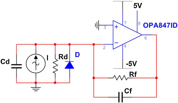
Fig. 1. Equivalent circuit model of the photodiode and transimpedance amplifier circuit.
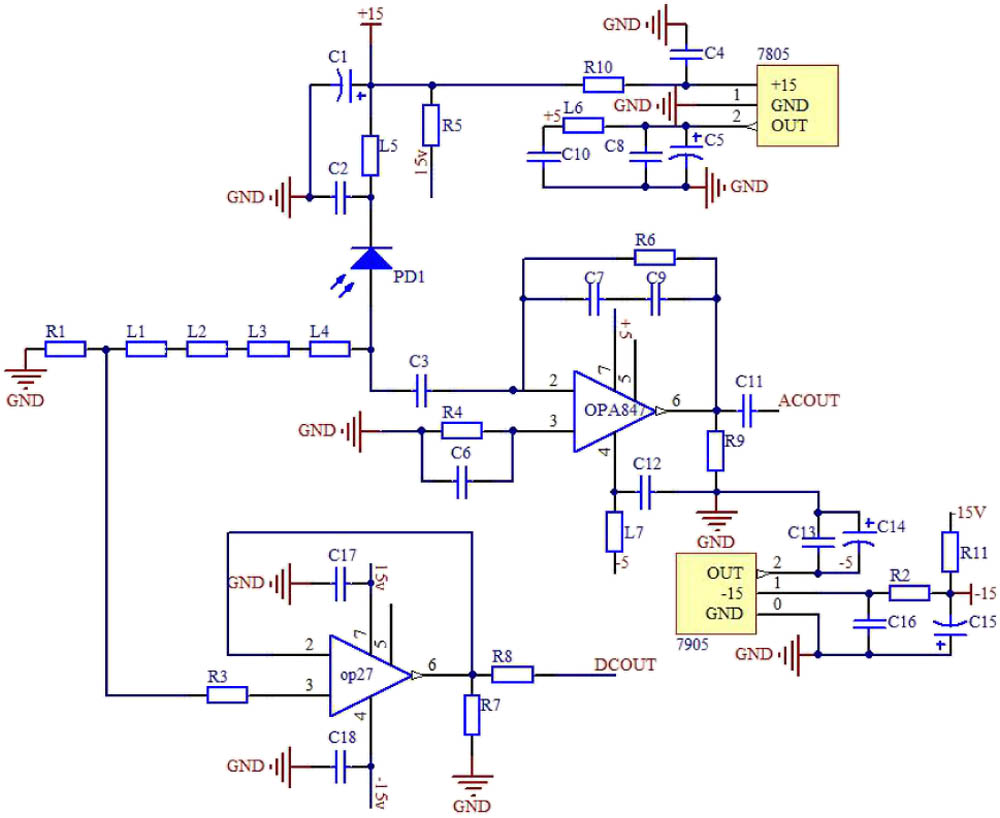
Fig. 2. Circuit schematic. Where, GND is ground. R f = R 6 = 3 kΩ R 4 = 3 kΩ R 1 = 100 Ω R 9 = 50 Ω R 3 = 1 kΩ C 3 = 1 nF C 7 = 0.5 pF C 9 = 0.5 pF C 6 = 10 pF L 4 = 330 μH L 2 = 100 μH L 1 L 3 − 15 V − 5 V
Fig. 3. Gain curve of the circuit. The gain peak is at about 82 MHz, and the intersection is − 3 dB
Fig. 4. Circuit input noise curve I Eq
Fig. 5. Calculated relative output power gain versus frequency. From bottom to top, the curves are the calculated relative electronics noise and output noise power when the optical input powers are 0.5, 1, 2, 4, 8, and 16 mW, respectively.
Fig. 6. Measured noise power of the laser with a different power. From the bottom curve to top, the lowest black curve is the background noise of the spectrum analyzer, and the blue one is the electronics noise of the photoelectric detector. The other curves are the output noise power with different laser powers.
|
Table 1. Parameters of the Photodetector with Different Input Optical Powers

Set citation alerts for the article
Please enter your email address
© Copyright 2018-2021 | Chinese Laser Press. All Rights Reserved 沪ICP备15018463号-20