Jiliang Qin, Zhihui Yan, Meiru Huo, Xiaojun Jia, Kunchi Peng, "Design of low-noise photodetector with a bandwidth of 130 MHz based on transimpedance amplification circuit," Chin. Opt. Lett. 14, 122701 (2016)
Copy Citation Text
A low-noise photodetector is a basic tool for the research of quantum information processing. We present a specially designed low-noise photoelectric detector with a bandwidth of 130 MHz, using a transimpedance amplification circuit. Based on the detailed calculation of the dependence on each parameter of the detector, a useful method of how to design a low-noise and broadband photodetector is provided. When the optical power is between 1.0 and 16 mW, the photodetector has a good linear response to the injected light. Its electronics noise power is below , which is within the whole bandwidth. When the incident light power is 2 mW, the output noise powers are 10.0, 8.0, and 6.0 dB higher than the corresponding electronics noise within the bandwidth of 1–50, 50–90, and 90–130 MHz, respectively, which is in good agreement with the theoretical prediction. Thus, this photoelectric detector could have good application prospects in quantum communication and an optical cavity locking system.
Quantum information is an important research topic in the quantum physics world. The development of more secure communications and faster computing has been achieved by taking the advantage of the quantum entanglement[1–3]. Quantum communication is one of the important subjects in quantum information research, because it can guarantee the security of information transmission from the basic principles of quantum mechanics. With the rapid development of quantum communication in recent years, the speed of quantum information transferring is also become faster and faster[4–6]. In order to realize the transmission of quantum information with a high speed in a continuous variable region, the high-efficiency detection with enough bandwidth of the light is an essential requirement. The noise of quantum communication is generally in the shot noise limit level, so a low-noise photodetector with a corresponding bandwidth is needed to realize the measurement of the light field in quantum communication research[7–9]. On the other hand, quantum entanglement is a basic resource for quantum information research[10], while the bipartite Einstein–Podolsky–Rosen (EPR) entangled state of light is usually obtained from a non-degenerate optical parametric amplifier (NOPA)[10–13] or two degenerate optical parametric amplifiers (DOPAs)[14] in the continuous variable region. With the further development of quantum information, the demand of the entanglement degree of the entangled state light field is higher and higher, which puts forward a more precise requirement of the locking cavity length of an NOPA or DOPA. In the Pound–Drever–Hall (PDH) locked and frequency-stabilized system, a sine signal of about 80 MHz is needed to modulate the laser[15], Thus, a broadband low-noise and high-gain photoelectric detector is needed to achieve the high-precision cavity lock in order to achieve a high-quality resonant cavity lock and reduce the impact of cavity locking in the generation system of the non-classical light field[16,17].
The shot noise current [alternating current (AC) of the photoelectric detector] and mean photo current [direct current (DC)] must be measured and recorded separately in some quantum optics experiments[18,19]. Currently, there are some commercial photodetectors with a bandwidth of about 100 MHz, but these detectors commonly amplify and output the DC and AC signal together, which would cause the detector to easily saturate when the light with optical power over 1 mW is injected into only one photodiode of the detector[20–24]. The main characteristic of our design is that there are several inductors, beads, and a resistor connecting in a series in the input port of the amplifier. The DC and AC signals are separated by an AC-coupling capacitor and then amplified respectively, thereby effectively preventing detector saturation at a low input power, and the gain of AC and DC signals can be independently adjusted according to the requirement of each experiment. When the optical power is between 1.0 and 16 mW, the photodetector has an excellent linear response of the injected light, and its electronic noise power is below , which is within the whole bandwidth. When the incident light power is 2 mW, the output noise powers are 10.0, 8.0, and 6.0 dB higher than the corresponding electronic noise within the bandwidth of 1–50, 50–90, and 90–130 MHz, respectively, which is in good agreement with our theoretical calculation. Thus, it has a strong applicability in the laboratory involving the relative research.
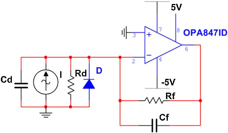
The photodiode is an important element in the photoelectric detector for realizing the conversion of the optical field to the photo current. Currently, the photo-intrinsic (PIN) diode and the avalanche photodiode (APD) are two kinds of commonly used semiconductor photoelectric detection devices, and they have different applications because of their characteristics. The PIN photodiode has no gain, but has a fast response. In the ideal case, the absorption of a photon will ideally produce an electron. The APD usually has a high gain, but has a larger current noise. Typically, the absorption of a photon generates a plurality of sub-carriers[25]. Since the detector we designed is used to detect the quantum noise of an optical field, we need to minimize its electronic noise. Therefore, we choose the PIN photodiode in our design. There are mainly three types of PIN photodiodes, including the Si PIN for the visible wavelengths, the InGaAs PIN for the near-infrared band, and the GaN PIN for the ultraviolet band[26,27]. In order to improve the quantum efficiency of the PIN photodiode, the light reflected by the device surface can be injected into the photodiode through assembling a resonant waveguide grating or utilizing a high-reflectivity mirror[28]. In the actual case, the PIN photoelectric diode usually has some junction capacitance and resistance. Thus, for facilitating the theoretical calculation and analysis, the photodiode can be modeled as connecting a current source , an ideal diode junction capacitance , and the dark resistance of photodiode in parallel, as shown in Fig. 1. The is usually very big, which can reach several dozens or hundreds of megohm, so it can generally be ignored[25]. The junction capacitance is representative of the photodiode’s positive–negative (PN) junction charge storage effect, which is related to the area and reverse bias voltage of the photodiode, , where is the zero-bias capacitance of the photodiode, is the reverse bias voltage, and is the built-in voltage of the PN junction[25]. Because has a great influence on the detector bandwidth, the value of must be small enough to achieve a detection bandwidth of several megahertz.
Sign up for Chinese Optics Letters TOC. Get the latest issue of Chinese Optics Letters delivered right to you!Sign up now
Figure 1.Equivalent circuit model of the photodiode and transimpedance amplifier circuit.
To design an amplification circuit which has a bandwidth of more than 100 MHz, the best way is to choose the transimpedance amplification circuit because it has the characteristics of a high bandwidth, and, thus, it is suitable for transferring a weak current signal into a voltage signal[29]. The diagram of the equivalent transimpedance preamplifier circuit based on OPA847 is shown in Fig. 1, where is the sum of the junction capacitance of the photodiode, the stray capacitance, and the amplifier’s common mode and differential mode input capacitance. is the feedback resistance. is the phase lead compensation capacitance. is small in general, only a few tenths to a few picofarads (pF), but it can eliminate the oscillation caused by the operational amplifier and . To make the operational amplifier work stably, we have to require [23,24]. Usually is about 0.1 pF of parasitic capacitance, so . Due to the influence of the parasitic capacitance, we can regulate empirically.
The main noise of the amplifier circuit includes operational amplifier noise, resistor thermal noise, and environmental noise. These noises will drown out a weak current signal and reduce the signal-to-noise ratio (SNR) of the detector, so we have to minimize this impact on the design of the low-noise detector. Fortunately, ambient noise can be reduced or eliminated by shading, electrical shielding, filtering circuit, power supply filtering, and other methods. Because the output signal of the photodiode is the current signal, we convert the circuit noise to the input current noise in order to facilitate the calculation. The resistor thermal noise equivalent input current noise is , and the circuit equivalent input noise current () at a different frequency () analysis is where is amplifier’s input current noise, and is amplifier’s input voltage noise[25,29].
Through the analysis of the stability, bandwidth, and noise, and in order to develop a wideband and low-noise photodetector, we must select an operational amplifier whose input noise current and input voltage noise is low and the Gain Bandwidth Product (GBP) is high. We choose the OPA847 produced by the TI Company as an AC output amplifier, and the low-noise chip OP27 as the DC output amplifier. If the detector is designed to stabilize the frequency by the PDH system, then S5973 (HAMAMATSU Company) is selected for the 795 nm laser, and G8376 (HAMAMATSU Company) is selected for the 1080 nm laser[30,31]. The photoelectric conversion efficiency of the G8376 is 0.67 A/W at the wavelength of 1080 nm. We should choose the PIN photodiodes with the higher quantum efficiency for efficiently measuring the quantum noise, like S5971, FD150, FGA-04, and so on. In the following experiments, we chose the G8376 to calculate and test.
The designed circuit of the generated photoelectric detector is shown in Fig. 2. The light is detected by the photodiode PD1 first, and then the photo current is divided to DC and AC signals by the inductors (L1-4) and a capacitor () for handling separately. The AC current signal flows through the inverting input terminal and is amplified by the OPA847 to measure the noise power of the injected light. and are the in-phase input impedance that should match the circuit to reduce the electronic noise and prevent the high-frequency oscillation. The DC signal is amplified by OP27 to measure the energy level of light. Under the condition of high frequency, the inductor is equivalent to an ideal capacitor and an ideal inductor in parallel and then in series with an ideal resistor because the real inductor usually has a parasitic capacitance in practice. We use several different values of inductors and beads in series because the main raw material of magnetic beads is ferrite, which has a high loss at the high-frequency region. When the current transmits through the beads, the impedance of the ferrite is small at a low frequency, while the ferrite can produce large attenuation in the high frequency[32]. Thus, the beads can not only suppress the effects of the high-frequency noise, but also increase the high-frequency impedance. and connected in series is used to increase the accuracy of . Different small value capacitors in series or parallel are used to meet the requirements in our experiment.
Figure 2.Circuit schematic. Where, GND is ground. , , , , , , , , , μ, μ, , and are chip beads. The 7805 and 7905 are power conversion modules, which can convert 15 and into 5 and .
The compromise between the gain and the bandwidth of the detector can be realized by changing the value of and properly adjusting . The current–voltage conversion gain of the photoelectric detector can be calculated[25] as where is the output voltage, is the input current, and is about 0.35 pF. The calculated gain frequency curve of the detector is shown in Fig. 3, and we find that the bandwidth of is 129 MHz. In the experiment for the measurement of quantum noise, the main requirement is that the gain should be as flat as possible in the whole bandwidth, and the gain curve will become flatter as the injection light increases because of the effect of the electronic noise in the high frequency. Thus, it can meet the requirements of the usual quantum optical experiments.
Figure 3.Gain curve of the circuit. The gain peak is at about 82 MHz, and the intersection is for the gain and 129 MHz for the frequency.
In order to meet the requirements of the quantum communication experiment, we also calculate the shot noise limit of the circuit. The photoelectric current is , where is the optical power, and is the photoelectric conversion efficiency of the photodiode, and the AC signal is , where is the electronic charge[16,33]. Therefore, the DC output is proportional to the laser power. Because the input current noise of OPA847 is (), and the input voltage noise is (), we can get the equivalent input noise current , and draw the curves of versus frequency, as shown in Fig. 4. The figure shows that the higher the frequency the higher the noise, so the SNR will become worse with an increasing frequency. If the values of are taken at the point of 30 and 100 MHz, we find that , and .
Figure 4.Circuit input noise curve versus frequency.
Table 1 gives the measurement of the DC output voltage Vdc of different optical powers P, the corresponding calculation of the AC signal , and the calculation of the SNR at several frequencies. We can see that the DC output of the designed photodetector has a linear response to the injected laser when its power is up to 16 mW, and the experimental results are basically consistent with the calculation results.
P (mW)
0.5
1
2
4
8
16
Vdc (mV)
33
65
132
262
522
1042
i (pA/Hz)
4.00
5.66
8.00
11.31
16.00
22.63
SNR(dB)30M
7.86
9.78
11.92
14.26
16.77
19.40
SNR(dB)100M
6.57
8.30
10.27
12.46
14.85
17.39
Table 1. Parameters of the Photodetector with Different Input Optical Powers
In order to check out the reliability of the actual results, we carry out the theoretical calculation of the noise spectrum. of the AC input signal is used as a reference input signal, and the relative output power gain versus frequency is theoretically calculated, as shown in Fig. 5. The bottom curve is the calculated relative electronics noise, and the other curves from the bottom to the top are the calculated output noise powers when the optical input powers are 0.5, 1, 2, 4, 8, and 16 mW, respectively. We find that the gain curve is relatively flat, and the SNR is relatively stable in the frequency range of 0–50 MHz. In the frequency range of 50–80 MHz, the gain curve increases, and the SNR decreases slightly. In the 80–150 MHz, the gain curve gradually decreases, while the SNR is significantly decreased.
Figure 5.Calculated relative output power gain versus frequency. From bottom to top, the curves are the calculated relative electronics noise and output noise power when the optical input powers are 0.5, 1, 2, 4, 8, and 16 mW, respectively.
Finally, we measure the AC output signal for the detector when different power lasers inject into the detector. The output noise power spectrum of the AC signal is recorded with a spectrum analyzer, as shown in Fig. 6. The lowest black trace in Fig. 6 is the recorded noise power of the spectrum analyzer. When we block the light injected into the photodiode, the electronics noise power of the photoelectric detector is measured, as shown in the red trace in Fig. 6. We find that the electronics noise power of the photodetector is below , which is within the whole frequency region. Then, the different power light is injected into the detector to measure the corresponding noise power, shown as the other trace in Fig. 6. In the low-frequency range, the noise of the laser we used in the experiment is far higher than the shot noise due to the relaxation oscillation. When the optical power is between 1.0 and 16 mW, the photodetector has a good linear response to the injected light. When the optical power is 2 mW, the output noise power is about 10.0, 8.0, and 6 dB higher than the corresponding electronics noise within the bandwidths of 1–50, 50–90, and 90–130 MHz, which is in good agreement with the theoretical calculation.
Figure 6.Measured noise power of the laser with a different power. From the bottom curve to top, the lowest black curve is the background noise of the spectrum analyzer, and the blue one is the electronics noise of the photoelectric detector. The other curves are the output noise power with different laser powers.
In conclusion, we design a low-noise photodetector with a 130 MHz practical bandwidth. When the injected optical power is 2 mW, the measured SNRs of the AC output are 10.2 and 8.0 dB at 30 and 100 MHz, respectively, which is in reasonable agreement with our theoretical prediction. Compared with other detectors with almost the same bandwidth, the noise level has been greatly improved. For example, the detector made by Chi et al.[20] has the same SNR as our detector, but the responding frequency region of ours has been enhanced. Although the commercial product C12702-03 made by Hamamatsu has a very high SNR, its noise level is also larger than ours. We also find that the junction capacitance of the photodiode affects the SNR and the bandwidth of the detector from the calculation. The smaller the , the better the two indexes. The and of the operational amplifier with a small magnitude can also reduce the SNR. In some situations, is more important than , such as in the lower frequency. However, has a more serious influence at a high frequency. So, the amplifier and photodiode must be chosen carefully in the design of the low-noise photodetector used in quantum optics research.
In this work, we provide a complete method for designing a photodetector that includes how to calculate the noise to meet our requirements and the key parameters when choosing the components. The parameters of the components are very important, and this detector is mainly used to detect the quantum noise of light. The photodetector has an almost flat gain in the bandwidth of 130 MHz, thus, we believe that in the future it can be used in continuous variable quantum communication with a transmission speed of about 100 MHz.
Jiliang Qin, Zhihui Yan, Meiru Huo, Xiaojun Jia, Kunchi Peng, "Design of low-noise photodetector with a bandwidth of 130 MHz based on transimpedance amplification circuit," Chin. Opt. Lett. 14, 122701 (2016)