
C. C. Gheorghiu, M. Cerchez, E. Aktan, R. Prasad, F. Yilmaz, N. Yilmaz, D. Popa, O. Willi, V. Leca. Fabrication of micrometre-sized periodic gratings in free-standing metallic foils for laser–plasma experiments[J]. High Power Laser Science and Engineering, 2022, 10(1): 010000e3
- High Power Laser Science and Engineering
- Vol. 10, Issue 1, 010000e3 (2022)
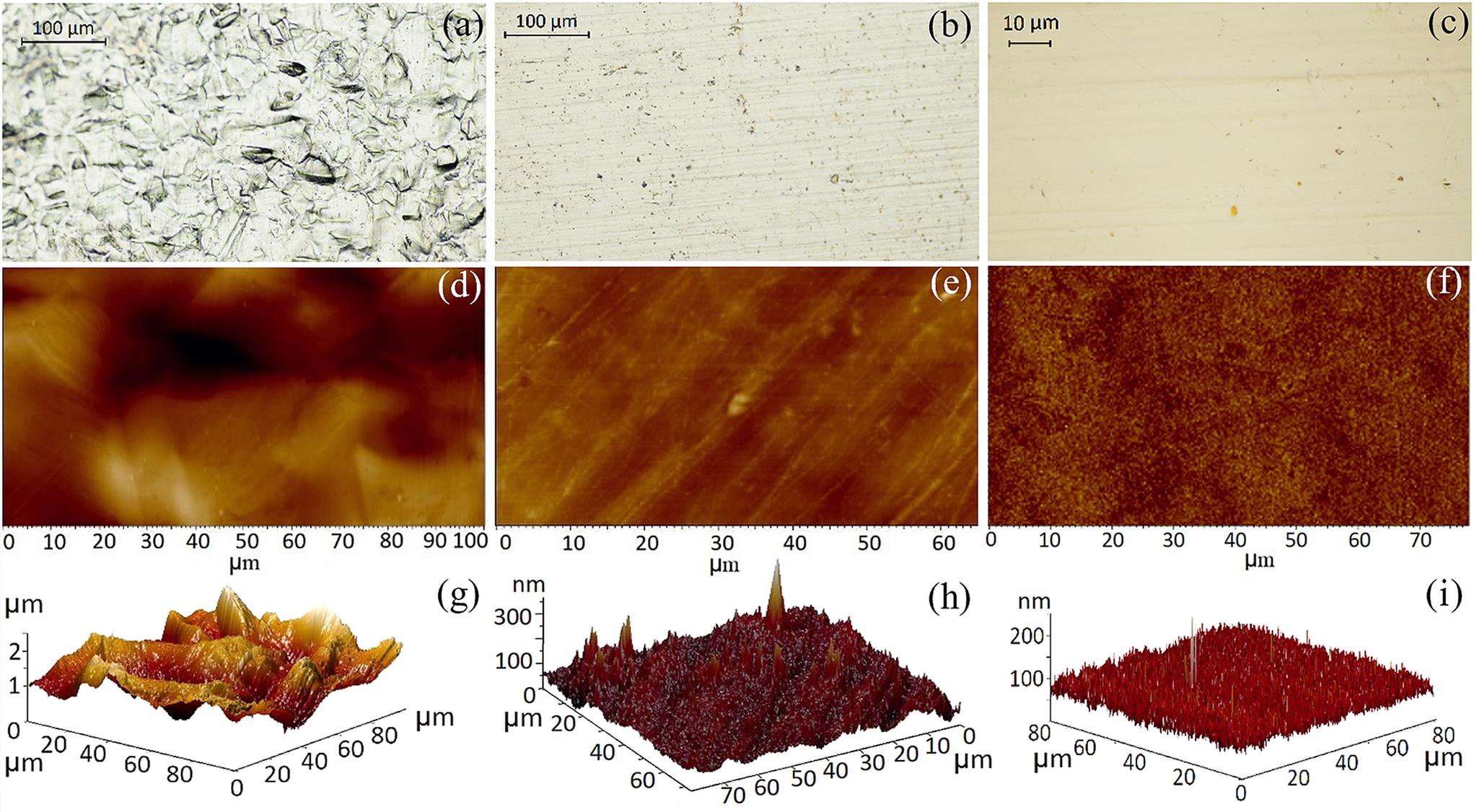
Fig. 1. (a)–(c) Optical images, (d)–(f) 2D AFM images and (g)–(i) 3D AFM images of Au foils: (a), (d), (g) as-received, (b), (e), (h) after cold rolling and (c), (f), (i) after surface cleaning by Ar-ion milling.

Fig. 2. (a)–(c) Optical images, (d)–(f) 2D AFM images and (g)–(i) 3D AFM images of Cu foils: (a), (d), (g) as-received, (b), (e), (h) after cold rolling and (c), (f), (i) after surface cleaning by Ar-ion milling.
Fig. 3. SEM images of micro-gratings using an unoptimized dry etching (Ar-ion milling) process: (a) Cu gratings, 9 min dry etching; (b) Au gratings, 20 min dry etching; (c) Cu gratings, 25 min dry etching; (d) Au gratings, 40 min dry etching; (e) Au gratings, 18 min dry etching + 10 min P1316 solution (RT); (f) Cu gratings, 9 min dry etching + 5 min P1316 solution (90°C); (g) Au gratings, 20 min dry etching, without foil cold rolling. For (f), dry etching was done perpendicularly to the surface, and at 45° to the sample normal for the rest.
Fig. 4. SEM images of grating patterns in (a) Cu and (b) Au foils obtained after the complete optimized fabrication process; darker parts correspond to non-etched areas and brighter parts to etched areas. Insets show an overview of the gratings. (c), (d) SEM and (e), (f) AFM images with (c), (e) Cu rectangular and (d), (f) Au sinusoidal (trapezoidal) shape gratings.
Fig. 5. Al holder with patterned Cu foil for assembly demonstration purposes: (a) back side; (b) front side with overlaid dark field optical image of the nine grated areas; (c) side view; (d) cross-section view.
Fig. 6. (a) Schematic of the experimental setup for the investigation of electron and proton acceleration by thin targets (gratings and planar surface). The IP stack is mounted on a motorized holder and can be vertically shifted. This allows access by a Thomson parabola spectrometer for proton acceleration measurements. (b) The top view of the IP stack shows the position relative to the target. (c) The IP stack sequence consists of IPs and aluminium filters of different thicknesses, which allows the detection of the electron spatial distribution for different energies. (d) A typical raw image of the IP signal. Here, θ and φ are the azimuthal and polar angles, respectively, used to describe the spatial distribution of the electrons.
Fig. 7. (a) Spatial distribution of the high-energy electrons accelerated by a thin planar Au FT foil (top) and a thin Au GT (bottom) irradiated by the laser pulse at 20° incidence angle. Here, the data correspond to IP2 (E > 1.2 MeV). (b), (c) The reconstructed angular distribution of the electrons for the planar foil (black) and grating (red) recorded by IP1 (E > 0.8 MeV) in similar interaction conditions as in (a) and for two laser incidence angles, 20° and 45°, respectively. (d) The distribution of the electrons as a function of emission angle for the planar foil (black) and grating (red) recorded by IP1 (E > 0.8 MeV) for the case of a 20° incidence angle.
Fig. 8. The total number of accelerated electrons with energies E > 0.8 MeV, including the front surface (FSE) and the rear surface (RSE) from gold FT and GT irradiated in similar conditions as in Figures 7 (b) and 7 (d).
Fig. 9. Experimental results of laser energy absorbed fraction by micro-gratings (GT) and flat surface targets (FT) for various laser incidence angles.
Fig. 10. The number of electrons accelerated along the front surface (SFE) within the azimuthal angle  as a function of laser angle of incidence (
E > 0.8 MeV). The values are normalized to the number of SFE electrons recorded for a planar thin foil at 0° laser incidence angle.
as a function of laser angle of incidence (Fig. 11. Raw images of proton and ion traces detected by a Thomson parabola/MCP setup recorded for Cu targets: (a) micro-grating (GT) and (b) thin flat (FT). Comparison of the reconstructed energy spectra of (c) protons and (d) C+4 ions for the two types of targets.
|
Table 1. RMS roughness obtained by AFM analysis of as-received and processed metallic foils.

Set citation alerts for the article
Please enter your email address
© Copyright 2018-2021 | Chinese Laser Press. All Rights Reserved 沪ICP备15018463号-20