• Chinese Optics Letters
  • Vol. 17, Issue 6, 062301 (2019)
Qingchen Yuan1, Liang Fang1, Qiang Zhao2, Yadong Wang1, Bo Mao1, Vladislav Khayrudinov3, Harri Lipsanen3, Zhipei Sun3、4, Jianlin Zhao1、*, and Xuetao Gan1、**
Author Affiliations
  • 1MOE Key Laboratory of Material Physics and Chemistry under Extraordinary Conditions, and Shaanxi Key Laboratory of Optical Information Technology, School of Science, Northwestern Polytechnical University, Xi’an 710072, China
  • 2Qian Xuesen Laboratory of Space Technology, China Academy of Space Technology, Beijing 100094, China
  • 3Department of Electronics and Nanoengineering, Aalto University, Espoo, FI-00076, Finland
  • 4QTF Centre of Excellence, Department of Applied Physics, Aalto University, Espoo, FI-00076, Finland
  • show less
    DOI: 10.3788/COL201917.062301 Cite this Article Set citation alerts
    Qingchen Yuan, Liang Fang, Qiang Zhao, Yadong Wang, Bo Mao, Vladislav Khayrudinov, Harri Lipsanen, Zhipei Sun, Jianlin Zhao, Xuetao Gan. Mode couplings of a semiconductor nanowire scanning across a photonic crystal nanocavity[J]. Chinese Optics Letters, 2019, 17(6): 062301 Copy Citation Text show less
    (a) Schematic diagram of an NW scanned across a PPC nanocavity along the lattice’s Γ−M direction. (b) Intensity distribution of the cavity’s fundamental mode. (c) ΣPx, Δλ, and η of the NW-PPC nanocavity versus the NW’s positions. (d) Q factor, Vmode, and ηQ/Vmode of the NW-PPC nanocavity versus the NW’s positions, where the red dashed lines indicate Q0 and Vmode0 of the bare nanocavity.
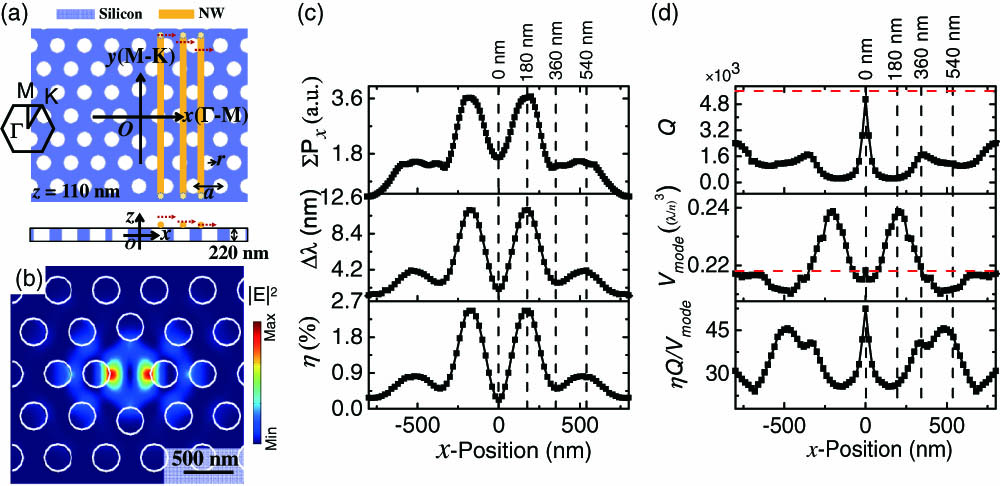
    Fig. 1. (a) Schematic diagram of an NW scanned across a PPC nanocavity along the lattice’s ΓM direction. (b) Intensity distribution of the cavity’s fundamental mode. (c) ΣPx, Δλ, and η of the NW-PPC nanocavity versus the NW’s positions. (d) Q factor, Vmode, and ηQ/Vmode of the NW-PPC nanocavity versus the NW’s positions, where the red dashed lines indicate Q0 and Vmode0 of the bare nanocavity.
    Mode intensity profiles and polarizations of electrical fields for NW positions of (a) 0 nm, (b) 180 nm, (c) 360 nm, and (d) 540 nm, where the intensities and polarizations are denoted by the colors and pink arrows.
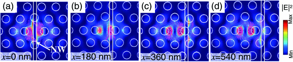
    Fig. 2. Mode intensity profiles and polarizations of electrical fields for NW positions of (a) 0 nm, (b) 180 nm, (c) 360 nm, and (d) 540 nm, where the intensities and polarizations are denoted by the colors and pink arrows.
    Simulation results when the NW scans along the lattice’s M−K direction. (a) ΣPy, Δλ, and η of the NW-PPC nanocavity versus the NW’s position. (b) Q factor, Vmode, and ηQ/Vmode of the NW-PPC nanocavity versus the NW’s position, where the red dashed line indicates the Q0 factor and Vmode0 of the bare nanocavity. (c1)–(c4) Mode intensity profiles and polarizations of electrical fields when the NW locates at (c1) y=0 nm, (c2) 160 nm, (c3) 280 nm, and (c4) 560 nm, respectively.
    Fig. 3. Simulation results when the NW scans along the lattice’s MK direction. (a) ΣPy, Δλ, and η of the NW-PPC nanocavity versus the NW’s position. (b) Q factor, Vmode, and ηQ/Vmode of the NW-PPC nanocavity versus the NW’s position, where the red dashed line indicates the Q0 factor and Vmode0 of the bare nanocavity. (c1)–(c4) Mode intensity profiles and polarizations of electrical fields when the NW locates at (c1) y=0nm, (c2) 160 nm, (c3) 280 nm, and (c4) 560 nm, respectively.
    Simulation results of coupling between the NW and the cavity’s second-order mode. (a) Mode intensity profile (top panel) and polarizations (bottom panel) of the cavity’s second-order mode. (b), (c) Δλ, Q factor, η, and ηQ/Vmode of the second-order mode versus the NW position when it is scanned along the (b) Γ−M and (c) M−K directions. The red dashed line indicates the Q0 factor of the bare nanocavity.
    Fig. 4. Simulation results of coupling between the NW and the cavity’s second-order mode. (a) Mode intensity profile (top panel) and polarizations (bottom panel) of the cavity’s second-order mode. (b), (c) Δλ, Q factor, η, and ηQ/Vmode of the second-order mode versus the NW position when it is scanned along the (b) ΓM and (c) MK directions. The red dashed line indicates the Q0 factor of the bare nanocavity.
    Experiment results of mode couplings in NW-PPC nanocavities when moving the NW along the lattice’s M−K direction. (a) AFM images of the NW-PPC nanocavities when the Al0.2Ga0.8As NW is gradually moved close to the cavity center. The scale bar corresponds to 500 nm. (b) The measured (dotted lines) and Lorentzian fitted (solid lines) reflection spectra of the (b1) fundamental and (b2) second-order resonant modes of the NW-PPC nanocavities with different NW positions. (c) Δλ of the (c1) fundamental and (c2) second-order modes versus the NW positions. (d) Q factors of the (d1) fundamental and (d2) second-order modes versus the NW positions, where the black (red) dashed lines represent the simulated (measured) Q0 factor.
    Fig. 5. Experiment results of mode couplings in NW-PPC nanocavities when moving the NW along the lattice’s MK direction. (a) AFM images of the NW-PPC nanocavities when the Al0.2Ga0.8As NW is gradually moved close to the cavity center. The scale bar corresponds to 500 nm. (b) The measured (dotted lines) and Lorentzian fitted (solid lines) reflection spectra of the (b1) fundamental and (b2) second-order resonant modes of the NW-PPC nanocavities with different NW positions. (c) Δλ of the (c1) fundamental and (c2) second-order modes versus the NW positions. (d) Q factors of the (d1) fundamental and (d2) second-order modes versus the NW positions, where the black (red) dashed lines represent the simulated (measured) Q0 factor.
    Qingchen Yuan, Liang Fang, Qiang Zhao, Yadong Wang, Bo Mao, Vladislav Khayrudinov, Harri Lipsanen, Zhipei Sun, Jianlin Zhao, Xuetao Gan. Mode couplings of a semiconductor nanowire scanning across a photonic crystal nanocavity[J]. Chinese Optics Letters, 2019, 17(6): 062301
    Download Citation