1MOE Key Laboratory of Material Physics and Chemistry under Extraordinary Conditions, and Shaanxi Key Laboratory of Optical Information Technology, School of Science, Northwestern Polytechnical University, Xi’an 710072, China
2Qian Xuesen Laboratory of Space Technology, China Academy of Space Technology, Beijing 100094, China
3Department of Electronics and Nanoengineering, Aalto University, Espoo, FI-00076, Finland
4QTF Centre of Excellence, Department of Applied Physics, Aalto University, Espoo, FI-00076, Finland
The position-dependent mode couplings between a semiconductor nanowire (NW) and a planar photonic crystal (PPC) nanocavity are studied. By scanning an NW across a PPC nanocavity along the hexagonal lattice’s Γ – M and M – K directions, the variations of resonant wavelengths, quality factors, and mode volumes in both fundamental and second-order resonant modes are calculated, implying optimal configurations for strong mode-NW couplings and light-NW interactions. For the fundamental (second-order) resonant mode, scanning an NW along the M – K (Γ – M) direction is preferred, which supports stronger light-NW interactions with larger NW-position tolerances and higher quality factors simultaneously. The simulation results are confirmed experimentally with good agreements.
Semiconductor nanowires (NWs) have emerged as an important building block for nanoscale photonics and optoelectronics due to the strong quantum confinement effects of charge carriers, exotic excitons, high refractive indices, etc.[1–3]. A variety of NW-based active photonic devices have been developed, including low-threshold nanolasers[4], nano-LEDs[5,6], high-sensitivity photodetectors[7–9], solar cells[10–12], and even multifunctional sensors[13]. Unfortunately, most of these active devices were implemented in a configuration where NWs were surface-illuminated by vertically single-passed light beams. It is a challenge to couple light into NWs effectively considering their nanometric cross-section, which hinders the improvements of device performances. Constructing nanophotonic structures consisting of NWs to assist light-NW coupling is desired.
Recently, planar photonic crystal (PPC) nanocavities have attracted great interests to integrate semiconductor NWs for enhancing their light–matter interactions and constructing optoelectronic devices. For instance, the first NW laser at the telecom band was realized by integrating an InP NW onto a silicon PPC nanocavity[14]. This geometry also enables a microwatts continuous-wave pumped second harmonic generation in an AlGaAs NW[15]. Compared to other optical cavities, the transverse confinements of resonant modes in PPC nanocavities are provided by the photonic bandgap of the periodic air holes, promising the design of nanoscale cavities with high-quality () factors[16]. It facilitates the resonant modes to have extremely high ratios of the factor to mode volume (), which provides strongly localized optical fields. The nanoscale mode distribution also enables its effective overlap with NWs. In the vertical direction of the PPC nanocavities, the resonant modes are confined via the total internal reflection of the subwavelength-thick slab. The combination of the modes’ high densities of electrical fields and their effective evanescent couplings with NWs indicates that the NW-PPC nanocavity could represent a reliable configuration to enhance light-NW interactions. In addition, PPCs have planar geometries for constructing NW-based optoelectronic devices, including laser diodes, photodetectors, and electro-optical modulators[14,17,18].
With the developed growth techniques of semiconductor NWs, it is possible to integrate them onto PPC nanocavities via the transfer-manipulation process or in-situ growth[15,19,20]. Because the NWs’ cross-sections and PPC nanocavities are both in the nanoscale, their spatial alignments would significantly determine the light-NW coupling strengths. On the other hand, an NW would break the cavity’s vertical total internal reflection due to the NW’s high refractive index, which might degrade the cavity’s Q via scattering loss. This extra scattering loss would lower the mode’s density of optical field as well as the light-NW interaction strength. A tradeoff between the mode-NW coupling strength and mode’s Q should be considered carefully in the NW-PPC nanocavity integration.
Sign up for Chinese Optics Letters TOC. Get the latest issue of Chinese Optics Letters delivered right to you!Sign up now
We herein study the varied mode couplings of an NW by scanning it across a PPC nanocavity and discuss the optimal NW location for effective light-NW interaction. The variations of resonant wavelengths (), factors, and mode-coupling efficiencies () are calculated when the NW is located at different positions, which indicate the strength of mode-NW couplings and light-NW interactions.
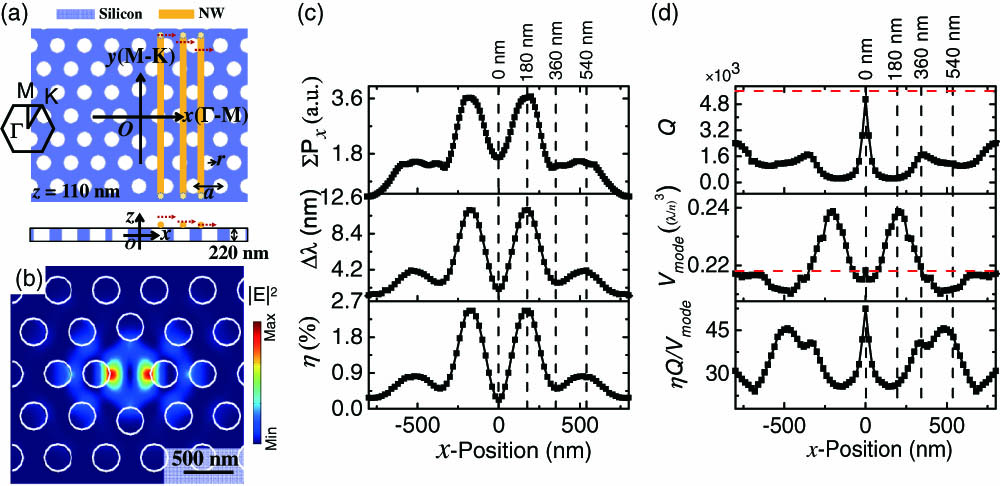
Figure 1(a) shows an NW scanned across a PPC nanocavity along the lattice’s direction. The coordinate system in the simulation model is displayed as well, which has an origin at the center of the cavity. The and axes correspond to the lattice’s and directions, respectively. Here, an H0 PPC nanocavity is employed, which is formed by shifting the four adjacent airholes outwards[21]. Compared to PPC cavities with missing air holes, the H0 PPC nanocavity has much smaller mode distribution and high- factor[21], allowing more effective light-NW couplings. The PPC is designed in a 220-nm-thick slab with a hexagonal lattice of air holes. The lattice constant is about , and the airhole radius is . In the cavity defect region, the four adjacent airholes are shifted by in the direction and in the direction, which enables high- resonant modes around the telecom band. An NW is then integrated onto the H0 PPC nanocavity, where the NW is a standard cylinder with a length of μ and a diameter of . The resonant modes of the integrated nanocavity are numerically simulated using a finite element technique (COMSOL Multiphysics). To be consistent with the experimentally fabricated device, the materials for the PPC nanocavity and NW are chosen as silicon and AlGaAs in the simulation model, which have refractive indices of and , respectively[15].
Figure 1.(a) Schematic diagram of an NW scanned across a PPC nanocavity along the lattice’s direction. (b) Intensity distribution of the cavity’s fundamental mode. (c) , , and of the NW-PPC nanocavity versus the NW’s positions. (d) factor, , and of the NW-PPC nanocavity versus the NW’s positions, where the red dashed lines indicate and of the bare nanocavity.
Before the NW’s integration, the fundamental resonant mode of the bare PPC nanocavity is obtained at the wavelength of with the factor of and of , where is the refractive index of silicon. The intensity profile is displayed in Fig. 1(b). The ultra-compact mode mainly distributes over two and three lattices along the and directions, respectively. Because the NW only has contact with the evanescent field of the cavity mode, the NW’s integration could be considered as a small perturbation to the resonant mode. According to the perturbation theory of the electromagnetic mode[16], the scanned NWs then induce shifts of the resonant wavelength (), which is described by
Here, is the electrical field of the resonant mode for the unperturbed (bare) PPC nanocavity, and is the NW-induced variation of the dielectric function. Hence, for resonant modes of the bare PPC nanocavity, it is worth calculating the optical power that would overlap with the NW, which indicates the mode-NW coupling strength. For the case that the NW is scanned along the direction ( direction), considering the NW’s one-dimensional structure, we calculate the optical power overlapping with the NW at different positions , as shown in the top panel of Fig. 1(c). It has the same trend as the mode distribution in Fig. 1(b).
After integrating the NW onto the PPC nanocavity, the representative parameters, including , factor, and of the abovementioned resonant mode, undergo significant changes when the NW scans to different positions across the cavity’s center. In the middle panel of Fig. 1(c), we plot the versus the NW’s positions. The resonant wavelengths all undergo red-shifts in comparison with that of the bare PPC nanocavity, which is consistent with the perturbation theory of Eq. (1) and distribution shown in the top panel of Fig. 1(c). has the largest value of 11.15 nm at , where the NW overlaps with the maximum node of the resonant mode. At the cavity’s center (), the weak coupling between the NW and optical power of the resonant mode only causes a . In the simulated modes of the integrated NW-PPC nanocavity, we could extract the mode-NW coupling efficiency directly by calculating the ratio of the optical power in the NW to that in the whole mode, i.e.,
The bottom panel of Fig. 1(c) plots the calculated result. While the NWs at different positions perturb the cavity mode differently, the position-dependent has the same trend as the variation of calculated from the bare cavity, which is shown in the top panel of Fig. 1(c). In brief, the most effective mode-NW coupling takes place at the positions where the optical power of the mode is the maximum.
To employ an optical cavity to enhance light-NW interaction, there are some other figures of merit that should be considered besides the mode-NW coupling efficiency . For instance, the resonant mode’s factor and imply the lifetime and spatial density of photons in the cavity, respectively. The intensity of the cavity mode is proportional to the factor of , which determines the light-NW interaction strength as well. We calculate the variations of the factor and for the NW-PPC nanocavities with different NW positions, as shown in the top and middle panels of Fig. 1(d), respectively, where the red dashed lines indicate the original factor and of the bare nanocavity. Due to the NW’s high refractive index of and the broken geometry symmetry, the integration of the NW would cause scattering loss for the resonant modes, which decrease the factor. The degraded factors have an opposite trend to the mode-NW coupling strength. When the NW locates at the cavity center, the factor has the largest value of 5100 due to the NW’s lower perturbation. Over the region where the optical power of the mode is large (), the factor decreases to values of . As will be discussed later, at this position, the NW induces an asymmetric mode distribution, which therefore yields more scattering loss.
Scanning the NW to different positions also varies the of the NW-PPC nanocavity between and , as shown in the middle panel of Fig. 1(d). Similar to the variations of the factors, the has less change when the NW locates around the cavity’s center and increases significantly when the NW is close to the mode’s maximum node. It could be attributed to the penetration of the optical field into the NW. However, when the NW moves further outward, the decreases to values smaller than that of the bare cavity. To explain this variation, we display the simulated resonant modes of the NW-PPC nanocavity with the NW at the characteristic positions in Fig. 2. When the NW locates at and 540 nm, the existence of the NW reshapes the resonant mode to induce more optical fields into the airholes, which therefore results in smaller .
Figure 2.Mode intensity profiles and polarizations of electrical fields for NW positions of (a) 0 nm, (b) 180 nm, (c) 360 nm, and (d) 540 nm, where the intensities and polarizations are denoted by the colors and pink arrows.
In the NW-PPC nanocavity, the optical intensity interacting with the NW is proportional to the mode’s factor, which is important for the NW-based electro-optic effect, nonlinear effect, Purcell effect, etc.[22,23]. Another factor determining the light-NW interaction is the portion of the resonant mode coupled with the NW, i.e., . We therefore would define the figure of merit to describe the light-NW interaction in the PPC nanocavity as . The function of the positions is plotted in the bottom panel of Fig. 1(d). To employ a PPC nanocavity to enhance the light-NW interaction, the optimal position of the NW is the cavity center, while the mode-NW coupling is strongest when the NW overlaps with the mode’s maximum node, i.e., .
Figure 2 displays the mode’s plane distribution of the NW-PPC nanocavities at , which is the plane through the NW’s center and actually shows the cavity’s evanescent field. These mode distributions could facilitate further explanations of the above results about the position-dependent , , , and . According to the mode-NW coupling results shown in Figs. 1(c) and 1(d), the NW’s positions are chosen as , 180, 360, and 540 nm to represent the special characteristics. In the intensity distributions shown in Figs. 2(a) and 2(c), the optical fields in the NW are almost null, i.e., the mode couples into the NW weakly. Hence, is less for these two cases. At the plane above the silicon slab, since a lower evanescent field is coupled into the NW, the mode is confined better by the total internal reflection, enabling a high- factor. For the cases of Figs. 2(b) and 2(d), more optical fields are confined into the NW, which therefore give rise to higher mode-NW coupling and lower factor. The varied mode-coupling behaviors of the NW at the four different positions are determined by the polarizations of the mode’s electrical fields. We denote the in-plane directions of the electrical field components and by using pink arrows. The density and length of the arrows imply the amplitude of the electrical field distribution. For the NW’s positions at and 360 nm, the electrical fields are mainly perpendicular to the NW, as shown in Figs. 2(a) and 2(b). According to the continuous boundary condition of the electromagnetic field, these perpendicular electrical fields are difficult to couple into the NW due to its high refractive index[8]. In contrast, when the NW moves to and 540 nm, the mode’s electrical fields are parallel to the NW, ensuring their effective couplings.
We then study the NW’s mode coupling by scanning it along the PPC lattice’s direction. Similar as the discussions for the case of the NW scanned along the direction, we plot the variations of , , , , , and when the NW locates at different positions, as shown in Figs. 3(a) and 3(b). The special NW positions with inflections of parameters are marked by the dark dashed lines at , 160, 280, and 560 nm. The mode’s intensity profiles and polarizations of electrical fields at these positions are displayed in Figs. 3(c1)–3(c4), which could be used to explain the variations in Figs. 3(a) and 3(b).
Figure 3.Simulation results when the NW scans along the lattice’s direction. (a) , , and of the NW-PPC nanocavity versus the NW’s position. (b) factor, , and of the NW-PPC nanocavity versus the NW’s position, where the red dashed line indicates the factor and of the bare nanocavity. (c1)–(c4) Mode intensity profiles and polarizations of electrical fields when the NW locates at (c1) , (c2) 160 nm, (c3) 280 nm, and (c4) 560 nm, respectively.
The position-dependent of the bare PPC nanocavity shows that the optical power is strongest at the cavity’s center (). However, and of the NW-PPC nanocavities indicate that the strongest mode-NW coupling happens when the NW locates at . It could be explained from the mode’s electrical field distributions shown in Figs. 3(c1)–3(c4). When the NW locates at the cavity’s center, most of the mode’s electrical fields are perpendicular to the NW, which significantly hinders their coupling and forms a valley bottom of [bottom panel of Fig. 3(a)]. However, is not a valley bottom [middle panel of Fig. 3(a)], implying that the NW perturbs the cavity mode strongly at the cavity’s center. In the middle panel of Fig. 3(b), there is a dip of the at . It implies that while the NW integration shifts the resonant wavelength strongly, most of the mode perturbation shapes the mode into the air around the NW, which is consistent with the weak mode-NW coupling due to the perpendicular electrical field. At , the electrical fields are parallel to the NW, as shown in Fig. 3(c3), which therefore couple with the NW effectively.
The NW-PPC nanocavity has the maximum factor when the NW locates at the cavity’s center, which actually approaches that in the bare PPC nanocavity. This non-degraded factor could be attributed to the weak mode-NW coupling as well as the mode symmetry maintained by the central NW integration, which is similar to that for the centrally located NW shown in Fig. 1. Compared to the case of the NW scanned along the direction, when the NW scans along the direction around the cavity’s center, the degradation of the factor is not very sudden, and the mode-coupling efficiency is lower. Even for the positions where is the maximum, the decreased factor still has values around 1800, which promises a variety of important applications relying on the mode’s narrow linewidth. Hence, scanning an NW along the cavity’s direction has a larger tolerance on the position around the cavity center, which also supports more efficient mode couplings over a broad spectral range. In addition, the NW scanning along the direction generates less variations over the , which is in a range of to , as shown in the middle panel of Fig. 3(b). We also plot in the bottom panel of Fig. 3(b) to present the position-dependent light-NW interaction. Compared to the corresponding results shown in Fig. 1(d), for the same resonant mode, the value of in the configuration of an NW orientating along the direction is much higher, and the maximum values almost flatly distribute over a spatial range of about 200 nm. More importantly, the factor maintains large detectable values over this wide spatial range, i.e., simultaneously promising high spectral resolutions in the NW-based devices.
The employed H0 PPC nanocavity has high-order resonant modes, which could also be employed to enhance light-NW interaction. As a representative, we herein present the mode coupling of a scanned NW with the cavity’s second-order resonant mode, as shown in Fig. 4. The second-order resonant mode usually has a far-field electrical field component perpendicular to that of the fundamental resonant mode[24], and it owns higher factors for applications of high-performance sensors[25]. In the simulation model, the NW and PPC nanocavity have the same parameters as those in the above section. The intensity profile and polarizations of the electrical fields for the second-order mode of the bare PPC nanocavity are shown in Fig. 4(a), which has the resonant wavelength of , , and . When the NW scans along the and directions, the varied figures of merit of the second-order mode are plotted in Figs. 4(b) and 4(c), respectively. Similar to the discussions for the fundamental mode, the variations of , , , and could be understood from the optical power distributions and electrical field directions of the mode overlapped with the NW. Specifically, the maximum is about 15.5 nm.
Figure 4.Simulation results of coupling between the NW and the cavity’s second-order mode. (a) Mode intensity profile (top panel) and polarizations (bottom panel) of the cavity’s second-order mode. (b), (c) , factor, , and of the second-order mode versus the NW position when it is scanned along the (b) and (c) directions. The red dashed line indicates the factor of the bare nanocavity.
For the two cases of NW scanned along the and directions, , which determines the strength of light-NW interaction, is the maximum when the NW locates around the cavity’s center for the former. For the latter situation, the maximum light-NW interaction happens when the NW locates at the cavity’s boundary, on account of the ultra-low factor. Hence, when coupling an NW with the second-order mode of the PPC nanocavity, it is preferred to locate the NW orientating along the direction at the cavity’s center, which could provide the strongest light-NW interaction and maintain the high- factor with a large position tolerance. This characteristic is opposite to that obtained when the scanned NW couples with the fundamental mode (shown in Figs. 1 and 3).
To validate the above simulation results, we experimentally slide an NW across a PPC nanocavity and monitor its modification on the resonant modes. The PPC nanocavity is fabricated in a silicon-on-insulator wafer with a 220-nm-thick top silicon layer[22]. With the combination of electron beam lithography, inductively coupled plasma dry etching, and wet chemical undercutting, an air-suspended PPC nanocavity is obtained, which is designed with the parameters used in the above simulations. An NW is employed to deposit onto the PPC nanocavity with an atomic force microscopy (AFM) technique[15]. The NW is pushed by the AFM tip precisely to certain positions with the monitoring of the whole AFM scanning image. By the above, for the fundamental (second-order) resonant mode, scanning an NW along the () direction is preferred; here, we just move the NW along the direction in order to experimentally verify the mode coupling. Figure 5(a) shows the AFM images while the NW moves to different positions on the PPC nanocavity along the direction. The first position of the NW is about 700 nm away from the cavity’s center, which is then successfully moved to 560, 400, 300, 260, 120, and 20 nm, respectively. From the profiles of the AFM images, the diameter of the NW is measured as 120 nm, and its length is about 6.4 μm.
Figure 5.Experiment results of mode couplings in NW-PPC nanocavities when moving the NW along the lattice’s direction. (a) AFM images of the NW-PPC nanocavities when the NW is gradually moved close to the cavity center. The scale bar corresponds to 500 nm. (b) The measured (dotted lines) and Lorentzian fitted (solid lines) reflection spectra of the (b1) fundamental and (b2) second-order resonant modes of the NW-PPC nanocavities with different NW positions. (c) of the (c1) fundamental and (c2) second-order modes versus the NW positions. (d) factors of the (d1) fundamental and (d2) second-order modes versus the NW positions, where the black (red) dashed lines represent the simulated (measured) factor.
The resonant modes of the bare and NW-PPC nanocavities are experimentally measured using a vertical microscope setup[26]. A tunable narrowband laser is employed as the excitation source, and the scattering signal from the nanocavity is measured by a photodiode, which gives rise to the scattering spectrum by tuning the laser’s wavelength. A cross-polarization configuration of the excitation light and scattering signal is used to improve the signal to noise ratio of the resonant mode. Resonant modes would be represented as narrowband peaks in the scattering spectra. Figures 5(b1) and 5(b2) show the acquired scattering peaks for the fundamental and second-order resonant modes from the NW-PPC nanocavities shown in Fig. 5(a). By fitting these peaks with Lorentzian functions, the and factors of the resonant modes are extracted. For the bare PPC nanocavity, the ( factors) of the two resonant modes are () and (), respectively. Due to the imperfections of the device fabrication, the and factors are derived from the above simulation results. Compared to the original and factors, we plot their variations versus the NW’s positions, as shown in Figs. 5(c) and 5(d). The corresponding simulation results are plotted as well. The variation trends of the and factors both have good agreements between the experiment and simulation results, which confirm the mode-NW coupling behaviors discussed above.
In conclusion, we demonstrate the mode couplings between an NW and resonant modes of a PPC nanocavity by scanning the NW across the cavity along the lattice’s and directions. The variations of , factor, and of the NW-PPC nanocavity are discussed carefully by referring to the cavity’s mode distribution and polarization of the electrical fields, which imply optimal NW positions for strong mode-NW couplings and light-NW interactions. For the fundamental (second-order) resonant mode, scanning an NW along the () direction is preferred, which supports stronger light-NW interactions when the NW locates over the cavity’s center. The NW’s position has a large tolerance for the device integration. Simultaneously, the high- factor could be maintained against the breaking of the total internal reflection. The semiconductor NWs’ unique optical and electrical properties endow them have advantages in photodetection, modulation, and light emission. Their mature growth and integration techniques make it possible to construct an NW-PPC nanocavity for enhanced light-NW interactions. Our work could provide guidelines for constructing NW-PPC nanocavity devices to enhance light-NW interactions and improve NW-based optoelectronic devices.