• Journal of Semiconductors
  • Vol. 44, Issue 4, 042801 (2023)
Ruoshi Peng*, Shengrui Xu*, Xiaomeng Fan*, Hongchang Tao*, Huake Su*, Yuan Gao*, Jincheng Zhang**, and Yue Hao*
Author Affiliations
  • Wide Bandgap Semiconductor Technology Disciplines State Key Laboratory, School of Microelectronics, Xi'dian University, Xi'an 710071, China
  • show less
    DOI: 10.1088/1674-4926/44/4/042801 Cite this Article
    Ruoshi Peng, Shengrui Xu, Xiaomeng Fan, Hongchang Tao, Huake Su, Yuan Gao, Jincheng Zhang, Yue Hao. Application of nano-patterned InGaN fabricated by self-assembled Ni nano-masks in green InGaN/GaN multiple quantum wells[J]. Journal of Semiconductors, 2023, 44(4): 042801 Copy Citation Text show less
    (Color online) Schematic representation of the process of preparing a nano-patterned InGaN layer by self-assembled Ni nano-masks.
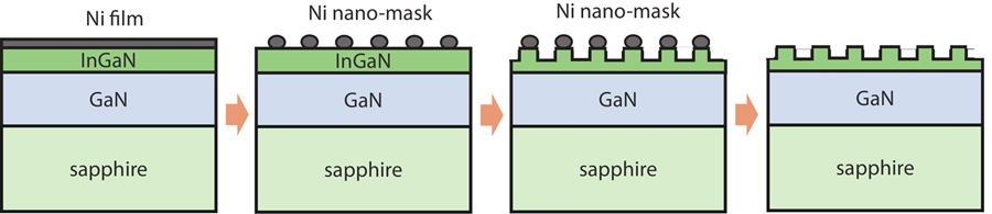
    Fig. 1. (Color online) Schematic representation of the process of preparing a nano-patterned InGaN layer by self-assembled Ni nano-masks.
    SEM images of the self-assembled Ni nano-masks using (a) 1 nm, (b) 3 nm, and (c) 5 nm deposited Ni film.
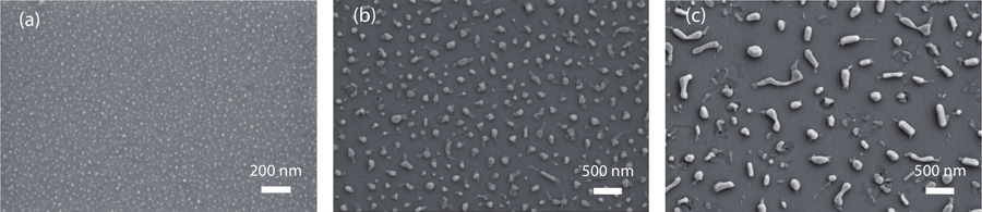
    Fig. 2. SEM images of the self-assembled Ni nano-masks using (a) 1 nm, (b) 3 nm, and (c) 5 nm deposited Ni film.
    SEM images of the nano-patterned InGaN of (a) Template I1, (b) Template I3, and (c) Template I5.
    Fig. 3. SEM images of the nano-patterned InGaN of (a) Template I1, (b) Template I3, and (c) Template I5.
    (Color online) The 5 × 5 µm2 AFM images of green InGaN/GaN MQWs structures of (a) Sample M0, (b) Sample M1, (c) Sample M3, and (d) Sample M5.
    Fig. 4. (Color online) The 5 × 5 µm2 AFM images of green InGaN/GaN MQWs structures of (a) Sample M0, (b) Sample M1, (c) Sample M3, and (d) Sample M5.
    (Color online) XRD results of Samples M0–M5. (a) GaN (002) reflection RC. (b) GaN (102) reflection RC. (c) Spectra of (002) ω–2θ scans.
    Fig. 5. (Color online) XRD results of Samples M0–M5. (a) GaN (002) reflection RC. (b) GaN (102) reflection RC. (c) Spectra of (002) ω–2θ scans.
    (Color online) PL spectra of Samples M0–M5 at room temperature.
    Fig. 6. (Color online) PL spectra of Samples M0–M5 at room temperature.
    (Color online) Schematic diagram of the light-emission path of the green InGaN/GaN MQWs (a) with untreated InGaN film and (b) with nano-patterned InGaN film.
    Fig. 7. (Color online) Schematic diagram of the light-emission path of the green InGaN/GaN MQWs (a) with untreated InGaN film and (b) with nano-patterned InGaN film.
    (Color online) CL images of (a) Sample M0, (b) Sample M1, (c) Sample M3, and (d) Sample M5.
    Fig. 8. (Color online) CL images of (a) Sample M0, (b) Sample M1, (c) Sample M3, and (d) Sample M5.
    ParameterSample M0Sample M1Sample M3Sample M5
    FWHM of (002) (arcsec)191.0142.3131.5132.8
    FWHM of (102) (arcsec)261.8239.8276.2326.8
    Dislocation density (108 cm−2)4.363.45 4.396.01
    Table 1. The XRD FWHM of GaN at (002) and (102) plane and the dislocation density of samples.
    Ruoshi Peng, Shengrui Xu, Xiaomeng Fan, Hongchang Tao, Huake Su, Yuan Gao, Jincheng Zhang, Yue Hao. Application of nano-patterned InGaN fabricated by self-assembled Ni nano-masks in green InGaN/GaN multiple quantum wells[J]. Journal of Semiconductors, 2023, 44(4): 042801
    Download Citation