
Kaikai Wang, Chao Wang, Haodong Shi, Zhuang Liu, Qiang Fu, Jiayu Wang, Yingchao Li, Huilin Jiang. Polarization Aberration Analysis and Compensation of Off-Axis Optical System with Digital Micro-Mirror Device[J]. Acta Optica Sinica, 2022, 42(16): 1611001
- Acta Optica Sinica
- Vol. 42, Issue 16, 1611001 (2022)
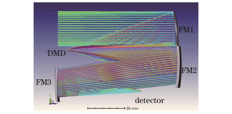
Fig. 1. Optical system structure diagram
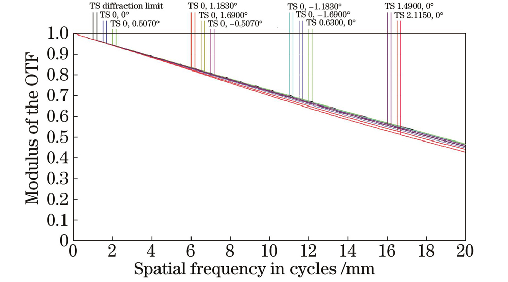
Fig. 2. MTF diagram
Fig. 3. Variations of amplitude and phase reflection coefficients for rs and rpwith incident angle. (a) Amplitude reflection coefficient; (b) phase reflection coefficient
Fig. 4. Schematic diagram of polarized light reflection on surface of DMD
Fig. 5. Variation trend of incident angle of light on DMD surface with fields of view
Fig. 6. Diattenuation of DMD surface and total system in fields of view of (1,-1) and (-1,1). (a)(b) Diattenuation of DMD surface; (c)(d) diattenuation of total system
Fig. 7. Retardance of DMD surface and total system in fields of view of (1,-1) and (-1,1). (a)(b) Retardance of DMD surface; (c)(d) retardance of total system
Fig. 8. Schematic diagram of compensation device setting
Fig. 9. Polarization aberration distributions of weak polarizer. (a) Diattenuation of LD; (b) retardance of LR
Fig. 10. System polarization aberration distributions after LD and LR compensations. (a) Diattenuation; (b) retardance
Fig. 11. Jones pupils. (a) Axx; (b) Axy; (c) ϕxx; (d) ϕxy; (e) Ayx; (f) Ayy; (g) ϕyx; (h) ϕyy
Fig. 12. Jones pupils of system after adding compensation device. (a) Axx; (b) Axy; (c) ϕxx; (d) ϕxy; (e) Ayx; (f) Ayy; (g) ϕyx; (h) ϕyy
Fig. 13. Stokes vector diagrams of object plane and image plane when horizontally polarized light is incident
|
Table 1. Parameters of optical system
| |||||||||||||||||||
Table 2. Maximum values of diattenuation and retardance at DMD surface and exit pupil in typical fields of view
| ||||||||||||||||||||||||
Table 3. Polarization aberrations of system before and after compensation under different wavelengths
|
Table 4. Accuracy of system polarization information acquisition at different wavelengths

Set citation alerts for the article
Please enter your email address
© Copyright 2018-2021 | Chinese Laser Press. All Rights Reserved 沪ICP备15018463号-20