• Infrared and Laser Engineering
  • Vol. 51, Issue 6, 20210648 (2022)
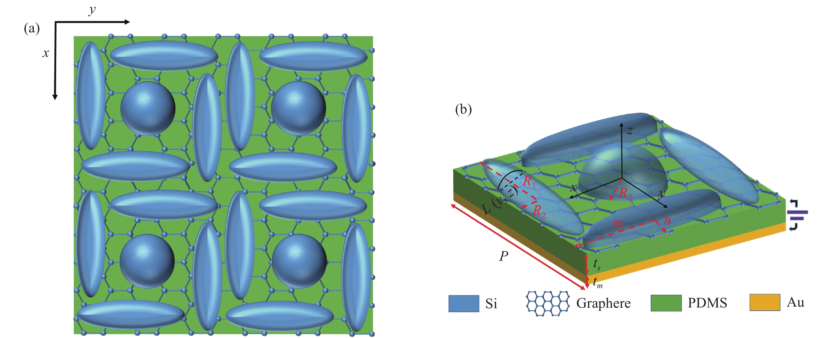
Xianrui Meng1、2, Ming Zhang1、2, Yupeng Xi1、2, Ruzhi Wang1、2, Changhao Wang1、2, and Bo Wang1、2
Author Affiliations
  • 1Institute of Advanced Energy Materials and Devices, Faculty of Materials and Manufacturing, Beijing University of Technology, Beijing 100124, China
  • 2Key Laboratory of Advanced Functional Materials, Ministry of Education, Faculty of Materials and Manufacturing, Beijing University of Technology, Beijing 100124, China
  • show less
    DOI: 10.3788/IRLA20210648 Cite this Article
    Xianrui Meng, Ming Zhang, Yupeng Xi, Ruzhi Wang, Changhao Wang, Bo Wang. Wideband terahertz metamaterial absorber for composite graphene/silicon hemispheres[J]. Infrared and Laser Engineering, 2022, 51(6): 20210648 Copy Citation Text show less
    (a) x-y plane diagram of the periodic structure of the broadband absorber;(b) 3 D schematic diagram of the absorber, where P=104 μm, R1=11 μm, R2= 38 μm, R3=26 μm, ts =15 μm, tm =2 μm
    Fig. 1. (a) x-y plane diagram of the periodic structure of the broadband absorber;(b) 3 D schematic diagram of the absorber, where P=104 μm, R1=11 μm, R2= 38 μm, R3=26 μm, ts =15 μm, tm =2 μm
    Absorption spectra of the proposed absorber with various values of the graphene chemical potential μ from 0 to 0.9 eV
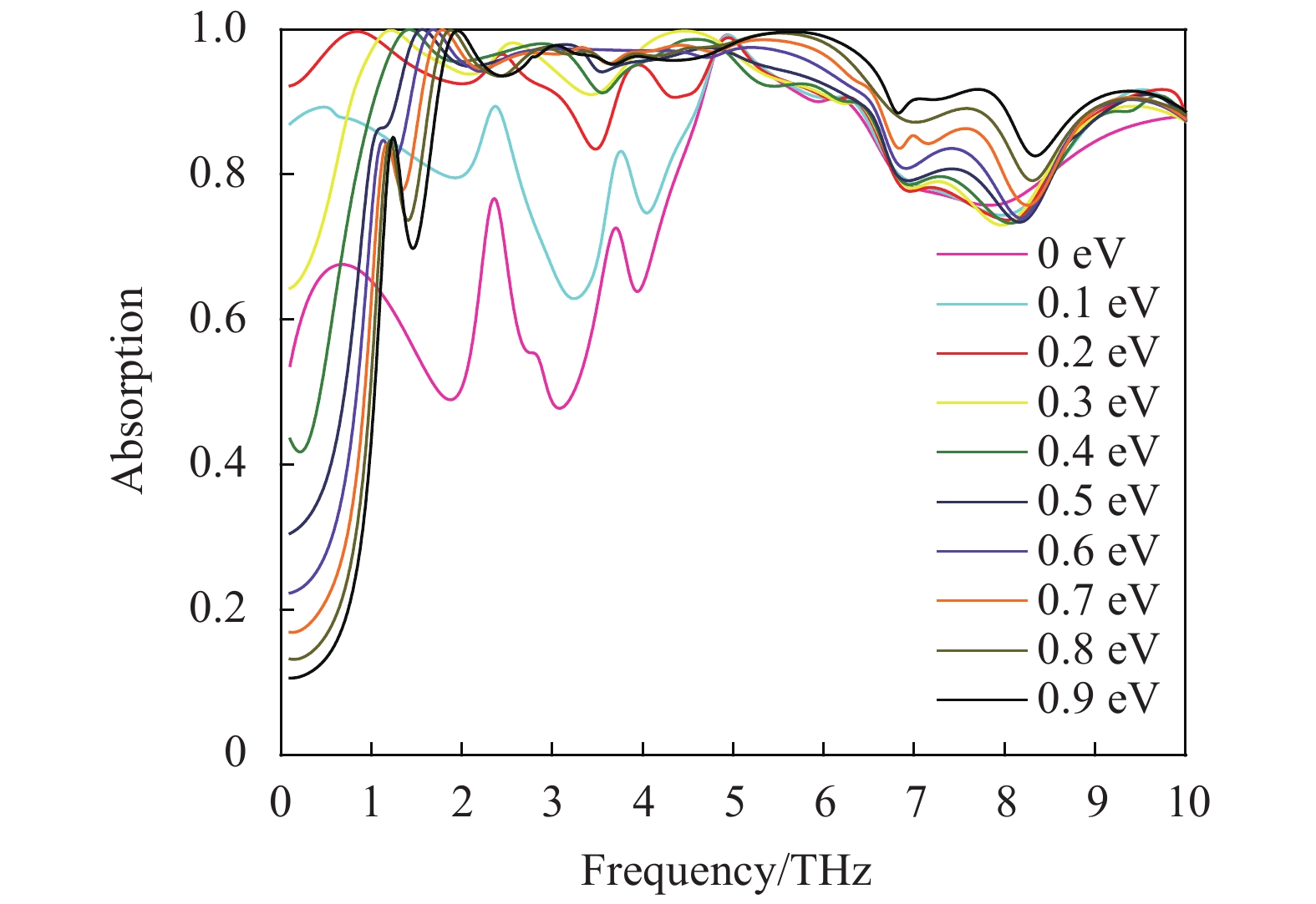
    Fig. 2. Absorption spectra of the proposed absorber with various values of the graphene chemical potential μ from 0 to 0.9 eV
    The electric field distributions (|E|) of the proposed absorber on the x–y plane with z = 50 nm at the different graphene chemical potential μ of (a) 0.1, (b) 0.2 and (c) 0.4 eV
    Fig. 3. The electric field distributions (|E|) of the proposed absorber on the xy plane with z = 50 nm at the different graphene chemical potential μ of (a) 0.1, (b) 0.2 and (c) 0.4 eV
    (a) Simulated absorption spectra of the proposed G-SemiEllip/SemiSphere absorber (red line) and four other absorbers with NN (black line), G-SemiSphere (blue line), G-SemiEllip (green line) and N-SemiEllip/SemiSphere (pink line)
    Fig. 4. (a) Simulated absorption spectra of the proposed G-SemiEllip/SemiSphere absorber (red line) and four other absorbers with NN (black line), G-SemiSphere (blue line), G-SemiEllip (green line) and N-SemiEllip/SemiSphere (pink line)
    The electric field distributions (|E|) of the proposed absorber on the x-y plane with z = 50 nm at the different frequencies of (a) 0.82 THz, and (b) 4.95 THz
    Fig. 5. The electric field distributions (|E|) of the proposed absorber on the x-y plane with z = 50 nm at the different frequencies of (a) 0.82 THz, and (b) 4.95 THz
    (a) The change rate of absorptivity with polarization angle (angle between electric field direction and y-axis) at oblique incident of TE wave; (b)-(c) The rate at which the absorptivity varies with the incidence angle θ (the angle between the incident direction and the z-axis) for oblique incidence of TE/TM waves
    Fig. 6. (a) The change rate of absorptivity with polarization angle (angle between electric field direction and y-axis) at oblique incident of TE wave; (b)-(c) The rate at which the absorptivity varies with the incidence angle θ (the angle between the incident direction and the z-axis) for oblique incidence of TE/TM waves
    Xianrui Meng, Ming Zhang, Yupeng Xi, Ruzhi Wang, Changhao Wang, Bo Wang. Wideband terahertz metamaterial absorber for composite graphene/silicon hemispheres[J]. Infrared and Laser Engineering, 2022, 51(6): 20210648
    Download Citation