
Huaile Nie, Shan Mao, Jianlin Zhao. Athermalization Design of Cooled Refractive-Diffractive Hybrid Dual-Band Infrared Optical System[J]. Acta Optica Sinica, 2023, 43(8): 0822025
- Acta Optica Sinica
- Vol. 43, Issue 8, 0822025 (2023)
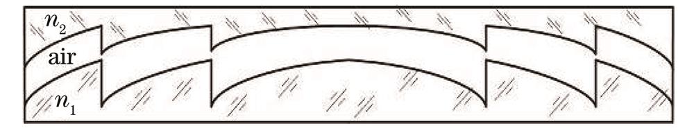
Fig. 1. Separated double-layer DOE

Fig. 2. Relationship among diffraction efficiency of double-layer DOE, incident angle, and wavelength
Fig. 3. Relationship between largest microstructure heights and design wavelengths. (a)
Fig. 4. Relationship between BIADE and design wavelengths
Fig. 5. Diffraction efficiency distribution
Fig. 6. Relationship among diffraction efficiency of double-layer DOE, temperature, and wavelength
Fig. 7. Solid model of infrared optical system
Fig. 8. Structure diagram of Dewar bottle
Fig. 9. MTF of optical system at -40, 20, and 60 ℃. (a) Middle waveband at -40 ℃; (b) long waveband at -40 ℃; (c) middle waveband at 20 ℃; (d) long waveband at 20 ℃; (e) middle waveband at 60 ℃; (f) long waveband at 60 ℃
Fig. 10. Field curvature and distortion of optical system at -40, 20, and 60 ℃. (a) Middle waveband at -40 ℃; (b) long waveband at -40 ℃; (c) middle waveband at 20 ℃; (d) long waveband at 20 ℃; (e) middle waveband at 60 ℃; (f) long waveband at 60 ℃
Fig. 11. Ensquared energy of optical system at -40, 20, and 60 ℃. (a) Middle waveband at -40 ℃; (b) long waveband at -40 ℃; (c) middle waveband at 20 ℃; (d) long waveband at 20 ℃; (e) middle waveband at 60 ℃; (f) long waveband at 60 ℃
|
Table 1. Design indexes of infrared optical system
|
Table 2. Parameters of infrared detector
| ||||||||||||||||||||||||||||||||||||||||||||||||||||||||||||||||||||||||
Table 3. Structure parameters of optical system
|
Table 4. Parameters of asphere surface
|
Table 5. Parameters of diffraction surface
| |||||||||||||||||||||||||||||||||||||||
Table 6. Maximum GEO and RMS radius of spot diagram in all fields of view at different temperatures

Set citation alerts for the article
Please enter your email address
© Copyright 2018-2021 | Chinese Laser Press. All Rights Reserved 沪ICP备15018463号-20