
Shuangshuang Wang, Chunyang Liu, Guozheng Wang, Xulei Qin. Effect of X-Ray Energy on X-Ray CsI(Tl) Scintillation Screen Based on Macroporous Silicon[J]. Laser & Optoelectronics Progress, 2022, 59(17): 1734001
- Laser & Optoelectronics Progress
- Vol. 59, Issue 17, 1734001 (2022)
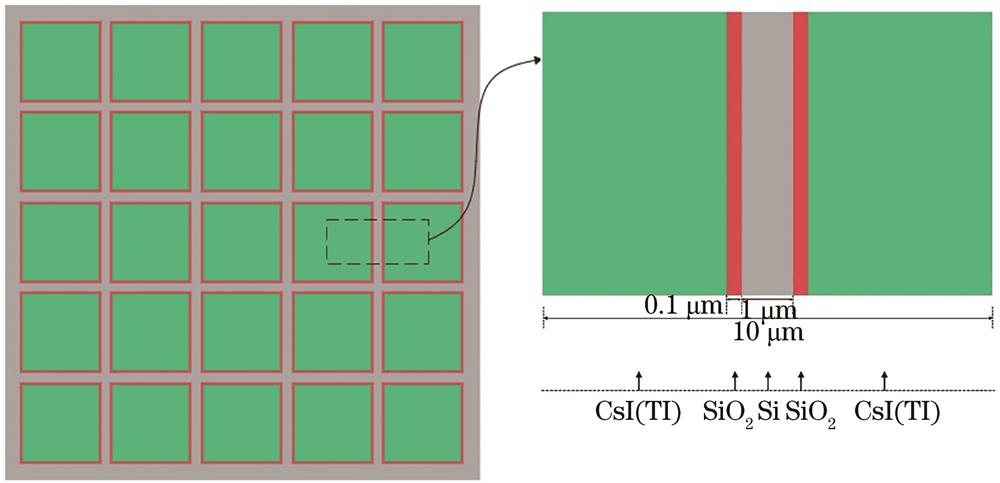
Fig. 1. Schematic diagram of X-ray CsI (Tl) scintillation screen model based on macroporous silicon
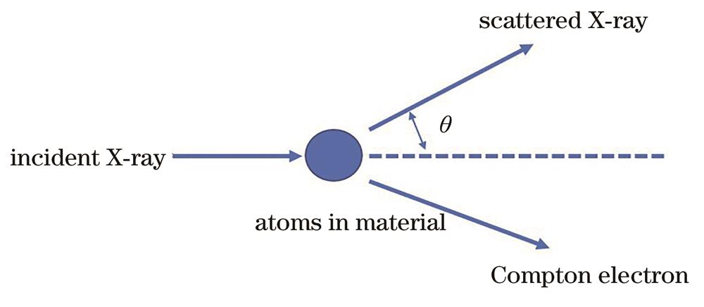
Fig. 2. Schematic diagram of Compton effect
Fig. 3. Schematic diagram of X-ray detection system
Fig. 4. X-ray energy versus number of output photons
Fig. 5. Simulation relationship between scintillation screen thickness and output photon number under different X-ray energies
Fig. 6. 50 pixel×50 pixel area grayscale photographs of X-ray images on 150-μm thick scintillation screen under different voltages. (a) Voltage is 80 kV; (b) voltage is 90 kV; (c) voltage is 100 kV; (d) voltage is 110 kV; (e) voltage is 120 kV; (f) voltage is 130 kV; (g) voltage is 140 kV; (h) voltage is 150 kV; (i) voltage is 160 kV
Fig. 7. 50 pixel×50 pixel area grayscale photographs of X-ray images on 310-μm thick scintillation screen under different voltages. (a) Voltage is 80 kV; (b) voltage is 90 kV; (c) voltage is 100 kV; (d) voltage is 110 kV; (e) voltage is 120 kV; (f) voltage is 130 kV; (g) voltage is 140 kV; (h) voltage is 150 kV; (i) voltage is 160 kV
Fig. 8. Curve diagram of relationship between tube voltage of X-ray source and average gray value of scintillation screen with different thicknesses
Fig. 9. Curve diagram of relationship between tube current of X-ray source and average gray value of scintillation screen with different thicknesses. (a) Thickness is 150 μm; (b) thickness is 310 μm

Set citation alerts for the article
Please enter your email address
© Copyright 2018-2021 | Chinese Laser Press. All Rights Reserved 沪ICP备15018463号-20