
Zhi Liu, Xiuli Li, Chaoqun Niu, Jun Zheng, Chunlai Xue, Yuhua Zuo, Buwen Cheng, "56 Gbps high-speed Ge electro-absorption modulator," Photonics Res. 8, 1648 (2020)
- Photonics Research
- Vol. 8, Issue 10, 1648 (2020)
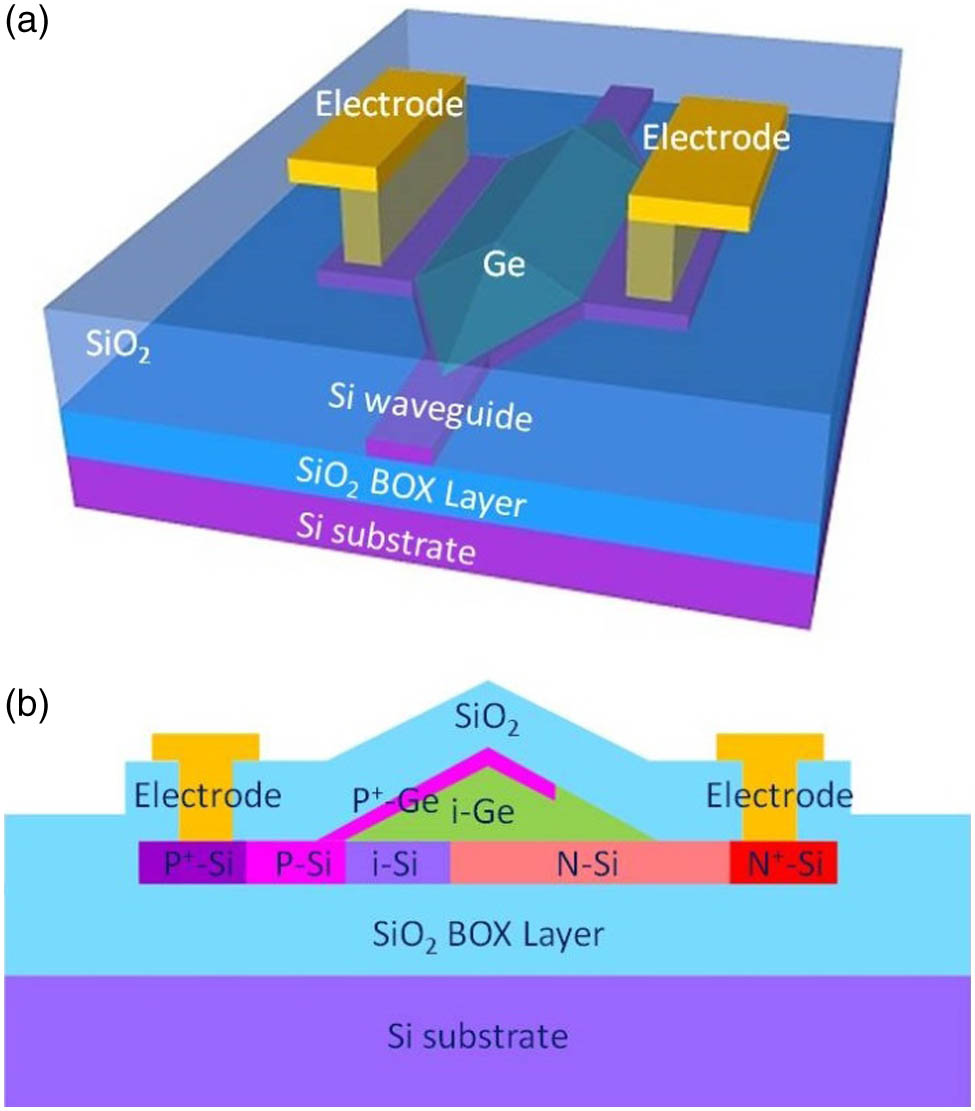
Fig. 1. (a) Schematic view of the EAM, (b) schematic cross-sectional structure of the EAM.

Fig. 2. (a) Cross-sectional optical field distribution of the EAM, (b) loss of the fundamental TE mode of the device’s structure, (c) electric field distribution in the EAM at − 2 V − 2 V
Fig. 3. (a) Top-view optical micrograph of the EAMs, (b) cross-sectional SEM image of the EAM.
Fig. 4. Typical I-V curves (with or without light input) and C-V curve of the EAM.
Fig. 5. (a) Optical transmission loss of the EAM (at various bias voltages) and without EAM, (b) IL and dc ER curves (at various bias voltages) of the EAM.
Fig. 6. S21 and S11 curves of the EAM at various bias voltages. The inset is the equivalent circuit model of the EAM.
Fig. 7. 56 Gbps eye diagrams of the EAM at 1600 and 1610 nm.
|
Table 1. Performance Comparison for Ge or GeSi EAMs


Set citation alerts for the article
Please enter your email address

© Copyright 2018-2021 | Chinese Laser Press. All Rights Reserved 沪ICP备15018463号-20