
Dongwei Zhuang, Xiaochuan Han, Yuxuan Li, Junfeng Song. Silicon-Based Optoelectronic Integrated Optical Phased Array[J]. Laser & Optoelectronics Progress, 2018, 55(5): 050001
- Laser & Optoelectronics Progress
- Vol. 55, Issue 5, 050001 (2018)
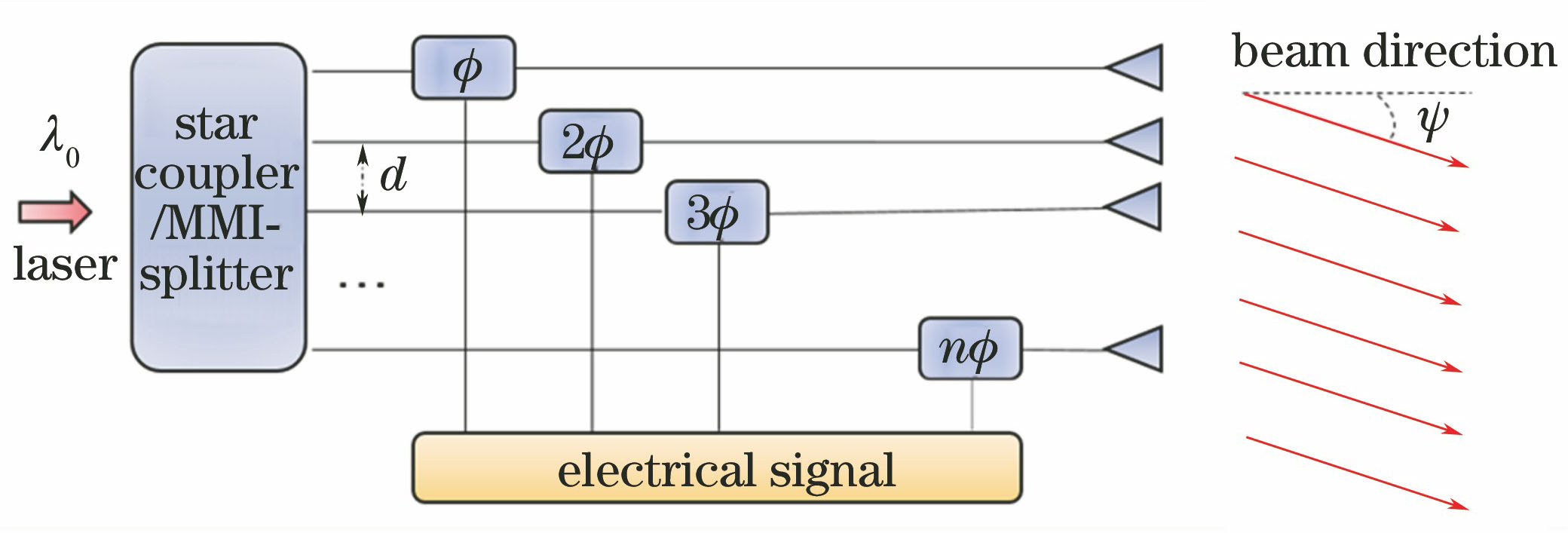
Fig. 1. Schematic of phase modulation optical phased array (OPA)
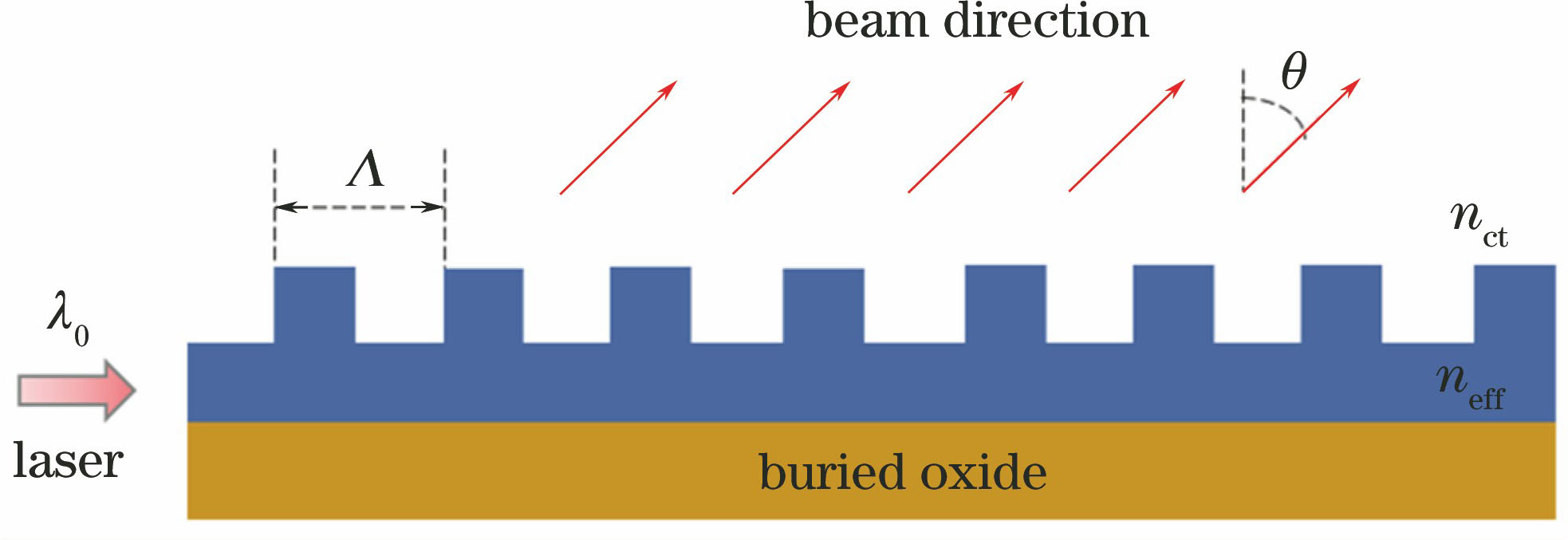
Fig. 2. Schematic of grating coupler for beam scanning
Fig. 3. Schematic of OPA integrated with on-chip laser
Fig. 4. (a) Schematic of large-scale nanophotonic phased array, the inset is close-up view of one antenna unit; (b) scanning electron microscope (SEM) of part of whole structure; (c) close-up SEM of one antenna unit
Fig. 5. Over arrangement of fully integrated beam scanner
Fig. 6. Schematic of hybrid-integrated OPA
Fig. 7. (a) Schematic of solid-state FMCW lidar system; (b) lidar chiplet on top of one dime; (c) optical micrograph of device
Fig. 8. (a) Schematic of simplified structure of device; (b) optical microscope image of star coupler;(c) tilted SEM image of emitter with removed cladding, the inset is schematic of emitter at a different angle
Fig. 9. Typical directional antenna radiation pattern in polar coordinate
Fig. 10. (a) Schematic of silicon nanophotonic coherent imager (NCI); (b) micro-photograph of NIC implemented by standard IME silicon-on-insulator process
|
Table 1. Specifications of one-dimensional scanning phased array
|
Table 2. Specifications of two-dimensional scanning phased array

Set citation alerts for the article
Please enter your email address
© Copyright 2018-2021 | Chinese Laser Press. All Rights Reserved 沪ICP备15018463号-20