Objective Gallium nitride (GaN) and its ternary alloys have drawn considerable attention because of their broad applications and promising market prospects for light-emitting devices. p-type doped GaN is an important part of GaN-based optoelectronic device structure. However, the applications of p-GaN are often limited by the low hole concentration and high resistivity. Until now, only Mg has been successfully employed as an effective and practical acceptor impurity in GaN for achieving useful p-type conduction. Post-growth treatment, such as thermal annealing, is required to activate the Mg acceptors in GaN in case of layers grown via metal-organic chemical vapor deposition (MOCVD). Further, there is convincing evidence that hydrogen passivates Mg acceptors in the as-grown state of the materials. An appropriate Mg doping concentration is required for obtaining high-quality GaN. The usage of a considerably high or low Mg doping concentration does not allow for a high hole concentration because of the self-compensation effect associated with heavy Mg doping. In addition, the dislocation density and the concentration of unintentionally doped impurities (e.g., carbon and oxygen) have an important effect on the resistivity of p-GaN. Overall, the compensation mechanisms and functions of the p-doped GaN and AlGaN materials must be clarified for their further development.
Methods A series of Mg-doped p-GaN films was grown in a vertical MOCVD system under different growth temperatures. An Aixtron 3×2 MOCVD system was used for growing p-GaN films. A 20-nm thick GaN buffer layer was initially grown at 540 ℃ on a sapphire substrate. Then, a 2-μm thick unintentionally doped GaN layer was grown by increasing the temperature to 1060 ℃. Subsequently, a series of 0.7-μm thick Mg-doped GaN layers was grown at 1000--1050 ℃. Each sample was annealed at 800 ℃ for 3 min under the same nitrogen environment for activating the Mg acceptors. Trimethylgallium (TMGa), ammonia (NH3), and Cp2Mg were used as sources of Ga, N, and Mg, respectively, when using MOCVD. All the conditions were maintained constant for each sample (A--E), except the growth temperature. X-ray diffraction was performed to confirm that the dislocation density in each sample was approximately identical. Further, the resistivity and hole concentration of each sample were measured using the room-temperature Hall method. In addition, the photoluminescence (PL) was measured and secondary-ion mass spectrometry (SIMS) was performed to study the compensation effect of the carbon impurities on p-GaN and its physical mechanism.
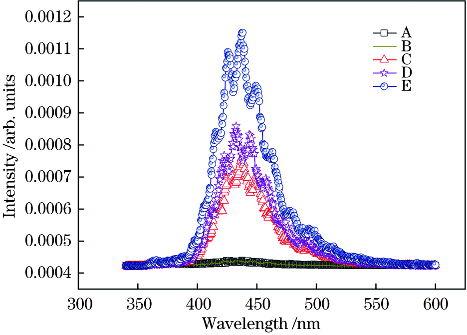
Results and Discussions The results obtained from the room-temperature Hall method (Table 1) indicate that the hole concentration increased and the resistivity decreased with the increasing growth temperature. To find possible causes for these phenomena, room-temperature PL spectra (Fig. 1) were obtained using a 325-nm laser beam excitation. The undulation of the PL spectral curves can be attributed to the interference caused by the Fabry-Perot effect owing to flat epitaxial films, which can be eliminated via a line-shape simulation treatment. Samples B, C, and D exhibited a blue luminescence (BL) band peak at approximately 430 nm (2.8 eV), whereas samples A and B did not exhibit such a peak. Detailed investigations have proven that the 2.8-eV BL is caused by donor-acceptor pair (DAP) recombination, where a strong BL peak indicates a high density of DAPs. A considerably high Mg doping concentration may induce a high concentration of DAPs, which can decrease the hole concentration and increase the resistivity. However, in this study, samples B, C, and D exhibited a high BL intensity but not the highest resistivity, implying that factors other than the self-compensation of Mg resulted in the high resistivity of GaN grown at low temperatures. By performing SIMS on samples B, C, and D (Fig. 2), we can observe that the carbon concentration in sample D was the lowest, implying that the concentration of carbon impurities considerably influences the resistivity of p-GaN by acting as a nonradiative recombination center and thereby decreasing the intensity of the BL band peak. Thus, the carbon impurities in p-GaN can form deep donors and compensate for the Mg acceptors, resulting in the deteriorated resistivity and poor mass of p-GaN. The experimental results presented in Table 2 indicate that the self-compensation effect of Mg in case of p-GaN growth was weaker at a lower growth temperature. However, a lower growth temperature can increase the density of carbon impurities, increasing the resistivity. Further, a higher growth temperature resulted in a stronger self-compensation effect and a lower carbon impurity concentration. The samples grown at high temperatures exhibited low resistivity despite the enhanced self-compensation effect of the Mg impurities, indicating that the compensation of carbon impurities played a more important role in p-GaN. Therefore, carbon impurities must be suppressed to obtain p-GaN materials with low resistivity and high hole concentrations. The p-GaN samples grown at high temperatures were of high quality because of their low concentrations of carbon impurities. High-quality p-GaN conduction layers are required for the growth of InGaN/GaN multiple quantum well optoelectronic devices. However, tradeoffs must be considered because the growth temperature of the top p-type GaN layer must not be considerably high to avoid thermal instability and the decomposition of the InGaN layers. It must be considerably lower than 1050 ℃ in a blue or green light-emitting device. Carbon impurities must be suppressed by regulating other growth conditions to obtain a high-quality p-type layer. Generally, the p-GaN layer in GaN/AlGaN multilayer devices must be grown at high temperatures.
Conclusions The effect of the growth temperature of heavily Mg-doped p-GaN films is studied based on the SIMS and PL measurements as well as the Hall method. Experimental results show that the self-compensation of the Mg impurity in p-GaN increased with the increasing growth temperature; however, its resistivity decreased. Further study indicated that the concentration of carbon impurity in the p-GaN sample grown at high temperatures was low. Carbon impurities can compensate for the Mg acceptor and increase the resistivity. The presented results indicate that the compensation of carbon impurities plays a more important role in the development of p-GaN films than the self-compensation of Mg. Thus, high-quality p-GaN films can be obtained by increasing the growth temperature appropriately to inhibit the incorporation of carbon impurities.