Weijie Mai, Luna Cui, Li Yu. Multimode-interference-based crossing for metal-insulator-metal waveguides[J]. Chinese Optics Letters, 2017, 15(3): 032301
Copy Citation Text
We report a waveguide crossing based on a multimode-interference (MMI) structure for metal-insulator-metal (MIM) waveguides. The MMI-based crossing comprises two orthogonal intersecting MMI waveguides that are connected to the single-mode input/output waveguide symmetrically. Single self-images are formed at the crossing center and output plane of the MMI waveguide, thereby mitigating the crosstalk and improving the throughput. The characteristics of the proposed MMI-based crossing are investigated with the finite element method of Comsol Multiphysics. The results show that the throughput reaches and the crosstalk is less than at the wavelength of 1550 nm.
Surface plasmon polaritons (SPPs) are regarded as promising candidates in future photonic integrated circuits because of their tight field confinements[1,2]. In particular, the metal-insulator-metal (MIM) waveguides based on SPPs has deep subwavelength field confinements and low bend loss, and thus, they have important applications in highly integrated photonic circuits[3–10]. Waveguide crossing, as a key component for the realization of high-density plasmonics interconnects in photonic circuits[11], requires high throughput and low crosstalk. However, it is known that a simple MIM crossing with subwavelength gap sizes splits the incoming pulse equally four ways because the subwavelength cross section of the input waveguide can excite the junction with a broad spectrum of plane waves[12–15] that do not meet the requirements of low crosstalk and high throughput in highly integrated photonic circuits. To decrease the crosstalk and enhance the forward transmittance of the waveguide crossing, Xiao et. al. designed simple cavity-based structures for MIM waveguides, and the reported throughput was about , with crosstalk below [16].
In conventional integrated optics, multimode-interference (MMI) -based devices have shown great value due to their advantages of low loss, wavelength insensitivity, and simple design and processing[17–19]. Recently, MMI-based plasmonic devices have also been demonstrated[20–23]. However, an MMI-based crossing for MIM waveguides has not been discussed. To combine the advantages of MIM waveguides and MMI-based devices, in this Letter, we propose an MMI-based crossing for MIM waveguides. The MMI-based crossing comprises two orthogonal intersecting MMI waveguides that are connected to the single-mode input/output waveguide symmetrically. In our design, only the two lowest-order even modes are excited inside the MMI section. The length of the MMI section is approximately twice the beat length of the two lowest-order even modes, yielding single self-images of the input field at the crossing center and MMI output plane. The first self-image forming at that cross center counteracts the wavefront expansion and thus mitigates the scattering loss and crosstalk. The second self-image forming at the MMI output plane ensures that high throughput can be obtained. The characteristics of the proposed MMI-based crossing are investigated with the finite element method (FEM) of Comsol Multiphysics. The results show that the throughput reaches and the crosstalk is less than at a wavelength of 1550 nm. These results are better than those mentioned in previous reports[16].
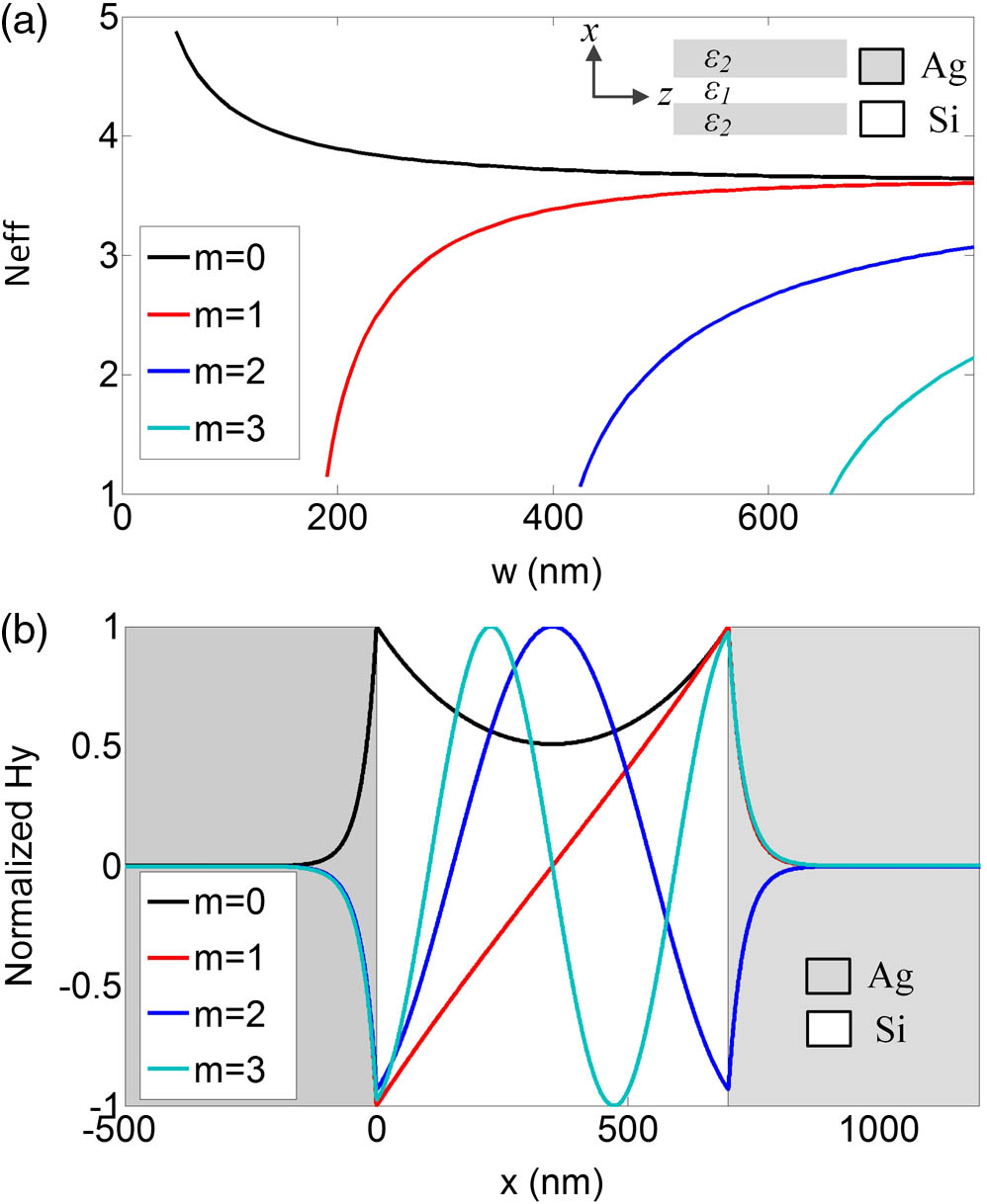
In order to use the MMI effect in MIM waveguides, the field distribution and propagation characteristics of the modes excited in the MIM waveguide are first investigated. The inset of Fig. 1(a) shows the fundamental structure of an MIM waveguide. The dispersion equation for the modes in the MIM waveguide is[23]where , , is the complex propagation constant of the mode excited in the MIM waveguide, , is the waveguide width, and and are the permittivities of the insulator and metal, respectively. is the order of the MIM waveguide mode, and . In the calculation, the dielectric and the metal are set to be Si and Ag, respectively. The permittivity of Si is . The permittivity of silver is estimated using the well-known Drude model[24]: , where the bulk plasma frequency, the collision rate, and the permittivity at an infinite frequency are set to , , and . Figure 1(a) illustrates the dispersion relation of the first four TM modes at a wavelength of using the FEM from COMSOL. It is clear that the fundamental mode does not exhibit a cutoff width. As the width increases, the MIM waveguide can support more modes. For example, the first-order mode of the waveguide appears when the width is larger than 200 nm, and more than four modes are excited in the MIM waveguide when the width is larger than 700 nm. Figure 1(b) illustrates the corresponding mode profiles. One can see that the even modes have no node for the field distributions () at the center of the MIM waveguide, while the odd modes have a node.
Sign up for Chinese Optics Letters TOC. Get the latest issue of Chinese Optics Letters delivered right to you!Sign up now
Figure 1.(a) Dispersion relation of MIM waveguide. (b) The field profile () of the first four TM modes in a 700 nm wide waveguide.
Based on the above-calculated results and analysis, an MMI-based crossing for an MIM waveguide, comprising two orthogonal intersecting MMI waveguides connected to the single-mode input/output waveguide symmetrically is designed as schematically shown in Fig. 2(a). Figure 2(b) shows the two-dimensional (2D) schematic structure of Fig. 2(a). The thicknesses of Si and Ag are much larger than the shin depth of the Ag layer. The influence of the thickness on the structure performance is little. In order to reduce the computational burdens, 2D simulations are performed, and the metal thickness is infinite in this 2D case. The width of the single-mode input and output waveguides is chosen to be 100 nm. To support higher-order modes, the widths of the MMI waveguides should be large enough. Here, the width of the MMI waveguide is chosen to be to support only the three lowest-order modes (i.e., , , and ), as shown in Fig. 1(b).
It should be noted that if the input position falls on the zero field point of a certain mode, the mode will not be excited[17]. So, in our design, only even modes (i.e., , ) can be excited in the MMI waveguide because the proposed device is symmetrical. According to the theory of MMI, the excited modes in the MMI waveguides will interfere with each other, and the input field forms self-images at periodic intervals along the propagation direction. The first self-image should be formed at a distance of away from the entrance of the MMI waveguide, where and are the propagation constants of the fundamental and second-order modes, respectively. To yield a first single self-image at the crossing center and a second single self-image at the MMI output plane, the length of MMI should be [25], where and are the real part of the effective indices of the fundamental and the second-order mode. They are calculated to be and [as shown in Fig. 1(a)], which correspond to . Figure 3 shows that the throughput and crosstalk of the device change from 2600 to 3000 nm. We can see that the lowest crosstalk and highest throughput can be obtained when the length of MMI waveguide is 2770 nm. The difference between the simulation value and theoretical value is due to the slight field distortion caused by the reflection at the end of the multimode waveguide and is acceptable. Therefore, according to the simulation results, the optimized length of the MMI waveguide is set to be to obtain the lowest crosstalk () and the highest throughput (). These results are better than those mentioned in a previous report (the throughput is about , with crosstalk below )[16].
Figure 3.Calculated throughput and crosstalk for MMI-based crossing as function of the MMI length . Here, and .
In order to have insight into the physical origin of the MMI effect in the proposed crossing, we plot the magnetic field distributions for the MMI-based crossing and the simple crossing without MMI waveguides. Figure 4(a) shows the magnetic field of our designed MMI-based crossing with and , which illustrates how the energy is fully transmitted forward through the crossing section. It clears that the input field couples to the first half of MMI section and forms the first single self-image at the cross center. After that, the field diverges again and re-forms another single self-image on the output plane. Although the lateral confinement is sharply altered in the crossing intersection region, the self-image property is little affected. In contrast, the field in the simple direct crossing couples into all four ports of the waveguide crossing, leading to a power-splitting scattering event, as shown in Fig. 4(b).
Figure 4.Field distribution () at for (a) MIM-based crossing and (b) direct crossing. (c) Throughput (solid lines) and crosstalk (dashed lines) for MIM-based crossing (blue lines) and direct crossing (red lines).
Figure 4(c) shows the throughput spectra and crosstalk spectra of the simple crossing without MMI waveguides and the MMI-based crossing with the same . For the direct cross, the forward throughput is about , almost same as the crosstalk. This result indicates that the simple crossing without MMI waveguides has low transmission and high crosstalk. For MMI-based crossing, the self-image forms at the cross center, which counteracts the wavefront expansion. The MMI effect enhances the forward throughput and mitigates crosstalk at the crossing. The throughput for the MMI-based crossing is improved by from that of the direct cross (from for the simple crossing without the MMI waveguide to for the MMI-based crossing), and the loss originates mainly from the metal absorption. The crosstalk for the MMI-based crossing is mitigated by (from for the direct crossing to for the MMI-based cross). It is also found that, for the crossing, the crosstalk is very low () over an bandwidth, and the throughput is relatively high () over such a broad band. These results show that the proposed MMI-based crossing is insensitive to the variation of the wavelength, which meets the requirements of integrated optical circuits.
Finally, the fabrication tolerance of the proposed MMI-based crossing is also discussed numerically. We assume that the MMI waveguide have the same width variation due to fabrication errors. Figure 5 shows the throughput spectra and crosstalk spectra when varies from to 90 nm. From Fig. 5, it can be seen that the throughput is not sensitive to the variation of . However, when the variation of is introduced, the influence on the crosstalk is obvious. The MMI-based crossing tolerates a width variation of for crosstalk and throughput , which alleviates the requirement of fabrication precision.
Figure 5.Fabrication tolerance of the proposed MMI-based crossing when there is an MMI waveguide width variation .
In conclusion, we propose an MMI-based crossing for an MIM waveguide. By forming the self-images of the input optical field at the crossing center and output plane, a crossing with high throughput () and low crosstalk () is achieved. The proposed MMI-based crossing has a broad band of for throughputs larger than and crosstalk less than . The MMI-based crossing tolerates a width variation of for crosstalk and throughput . These results can be useful for future integrated optical circuits.
Weijie Mai, Luna Cui, Li Yu. Multimode-interference-based crossing for metal-insulator-metal waveguides[J]. Chinese Optics Letters, 2017, 15(3): 032301