• Acta Photonica Sinica
  • Vol. 50, Issue 12, 1228002 (2021)
Peng SUN1、2, Jianyu FU1、2、*, Gaobo XU1、2, Mingzheng DING1, Qionghua ZHAI1, Huaxiang YIN1、2, and Dapeng CHEN1、2
Author Affiliations
  • 1Key Laboratory of Microelectronics Devices & Integrated Technology, Institute of Microelectronics of Chinese Academy of Sciences, Chinese Academy of Sciences, Beijing 100029, China
  • 2University of Chinese Academy of Sciences, Beijing 100049, China
  • show less
    DOI: 10.3788/gzxb20215012.1228002 Cite this Article
    Peng SUN, Jianyu FU, Gaobo XU, Mingzheng DING, Qionghua ZHAI, Huaxiang YIN, Dapeng CHEN. Research on Structure Simulation of Silicon Pixel Sensor Guard Ring for Advanced Light Source[J]. Acta Photonica Sinica, 2021, 50(12): 1228002 Copy Citation Text show less
    Schematic of the edge position of the sensor
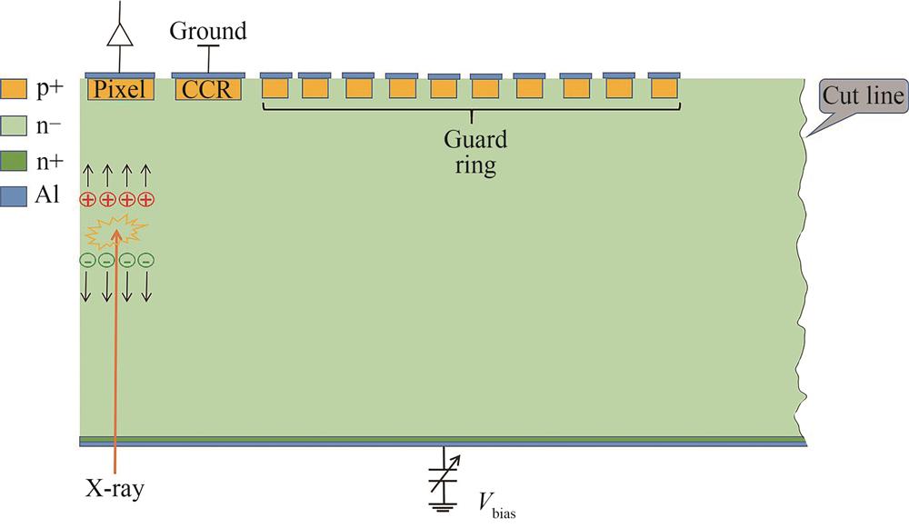
    Fig. 1. Schematic of the edge position of the sensor
    Sensor process flow chart
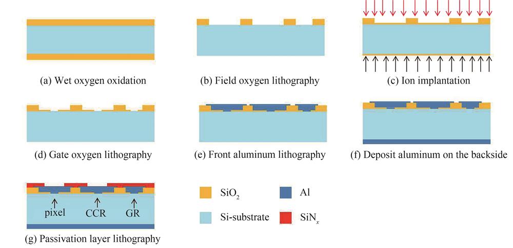
    Fig. 2. Sensor process flow chart
    Sensor edge simulation model
    Fig. 3. Sensor edge simulation model
    Pixel and current collecting ring dark current
    Fig. 4. Pixel and current collecting ring dark current
    Current density distribution diagram of equidistant guard ring structure (2 000 V bias)
    Fig. 5. Current density distribution diagram of equidistant guard ring structure (2 000 V bias)
    Surface potential distribution (2 000 V bias)
    Fig. 6. Surface potential distribution (2 000 V bias)
    Surface electric field intensity distribution (2 000 V bias)
    Fig. 7. Surface electric field intensity distribution (2 000 V bias)
    Al overhang of structure 2
    Fig. 8. Al overhang of structure 2
    Current collecting ring and pixel leakage under different Al overhang structures
    Fig. 9. Current collecting ring and pixel leakage under different Al overhang structures
    Surface potential distribution under different Al overhang structures (2 000 V bias)
    Fig. 10. Surface potential distribution under different Al overhang structures (2 000 V bias)
    Surface electric field distribution under different Al suspension structures (2 000 V bias)
    Fig. 11. Surface electric field distribution under different Al suspension structures (2 000 V bias)
    Leakage of current collecting ring under different number of guard rings
    Fig. 12. Leakage of current collecting ring under different number of guard rings
    Electric field distribution near the current collecting ring junction area (1 000 V bias)
    Fig. 13. Electric field distribution near the current collecting ring junction area (1 000 V bias)
    Surface potential distribution of different guard ring structures (1 000 V bias)
    Fig. 14. Surface potential distribution of different guard ring structures (1 000 V bias)
    The breakdown voltage of the current collecting ring changes with the number of guard rings
    Fig. 15. The breakdown voltage of the current collecting ring changes with the number of guard rings
    Distribution of potential drop near the first guard ring (1 000 V bias)
    Fig. 16. Distribution of potential drop near the first guard ring (1 000 V bias)
    Substrate thickness/μmSubstrate resistivity/(Ω·cm)Crystal orientationActive area injection width/μm
    PixelCCRGR
    5005 000<100>18020025
    Table 1. Substrate parameters and some structural parameters used in the simulation model construction
    Peng SUN, Jianyu FU, Gaobo XU, Mingzheng DING, Qionghua ZHAI, Huaxiang YIN, Dapeng CHEN. Research on Structure Simulation of Silicon Pixel Sensor Guard Ring for Advanced Light Source[J]. Acta Photonica Sinica, 2021, 50(12): 1228002
    Download Citation