
Peiru Zhang, Huan Liu, Jiaxing Hu, Lier Deng. Synthesis of Monolayer MoS2(1-x)Se2x Alloy and Photoelectric Properties of MoS2(1-x)Se2x (x=0. 25) Field-Effect Transistor[J]. Acta Optica Sinica, 2022, 42(16): 1616001
- Acta Optica Sinica
- Vol. 42, Issue 16, 1616001 (2022)

Fig. 1. Growth diagram of monolayer MoS2(1-x)Se2x prepared by chemical vapor deposition
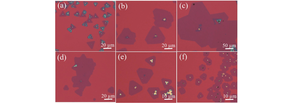
Fig. 2. Morphology of monolayer MoS2(1-x)Se2x alloy grown by different mSe/mS under optical microscope. (a) mSe/mS = 1/11; (b) mSe/mS = 1/5; (c) mSe/mS = 1/3; (d) mSe/mS = 1/2; (e) mSe/mS = 5/7; (f) mSe/mS = 1/1
Fig. 3. AFM image at junction of monolayer MoS2(1-x)Se2x and SiO2/Si substrate
Fig. 4. Relationship between size of monolayer MoS2(1-x)Se2x and mSe/mS
Fig. 5. SEM-EDS images of monolayer MoS2(1-x)Se2x alloy with different components. (a) x=0.23; (b) x=0.24; (c) x=0.25; (d) x= 0.40; (e) x=0.41; (f) x=0.42
Fig. 6. Relationship between x component value and mSe/mS in monolayer MoS2(1-x)Se2x
Fig. 7. Raman spectra and statistical analysis of Raman peak positions of monolayer MoS2(1-x)Se2x alloy with different components. (a) Raman spectra; (b) statistical analysis of Raman peak positions
Fig. 8. PL spectra, statistical analysis of peak positions and deviation diagram of band gap of monolayer MoS2(1-x)Se2x alloy with different components. (a) PL spectra of monolayer MoS2(1-x)Se2x alloy with different components; (b) relationship between wavelength position of PL peak of each component alloy and component value x; (c) deviation diagram between band gap value converted by PL spectrum and band gap value calculated according to band gap relationship
Fig. 9. Device structure and photoelectric test diagram of monolayer MoS2(1-x)Se2x FET. (a) Structural diagram of device; (b) I-V curve of monolayer MoS2(1-x)Se2x (x=0.25) device under darkness; (c) photoresponse current curves of monolayer MoS2(1-x)Se2x (x= 0.25) device excited by 520, 780, 980 nm laser; (d) enlarged view of photoresponse current curves at arrow mark in Fig. 9(c)
|
Table 1. Experimental detailed growth parameters
|
Table 2. Comparison of Raman characteristic peaks and PL emission peak positions of monolayer alloy with different components with literature results
|
Table 3. Comparison between performance test results of FET prepared in this paper and test results in literatures

Set citation alerts for the article
Please enter your email address
© Copyright 2018-2021 | Chinese Laser Press. All Rights Reserved 沪ICP备15018463号-20