
Xiaojie Liao, Suying Lin, Bing Han. Evolution mechanism of transient optical properties of ultrafast laser-induced monocrystalline silicon[J]. Infrared and Laser Engineering, 2022, 51(2): 20210907
- Infrared and Laser Engineering
- Vol. 51, Issue 2, 20210907 (2022)
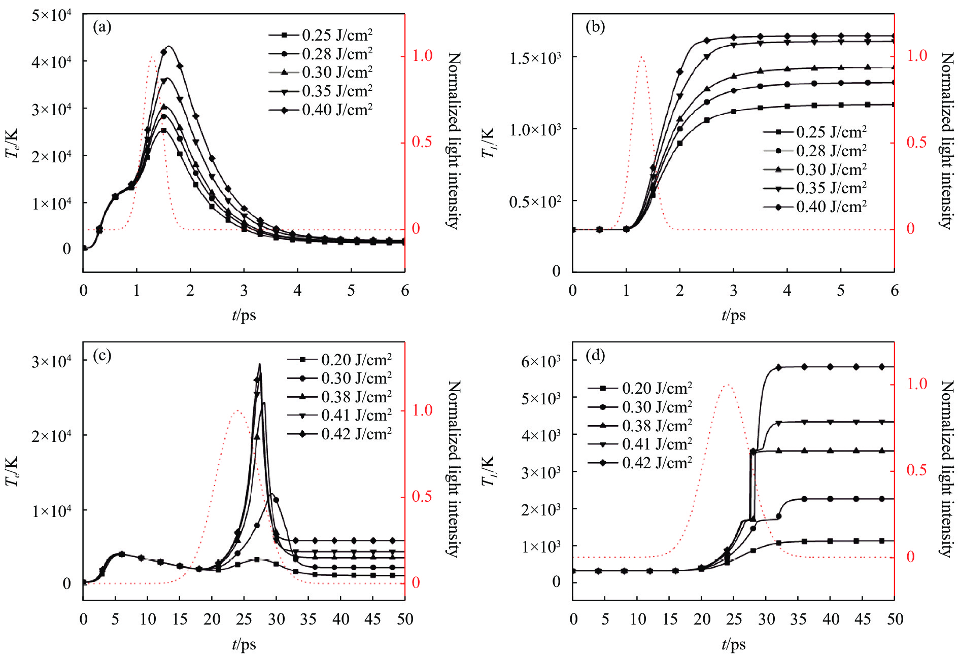
Fig. 1. Variation of electron temperature with time (a) and lattice temperature with time (b) under subpicosecond laser irradiation with energy density of 0.25, 0.28, 0.30, 0.35, 0.40 J/cm2 and pulse width of 430 fs; Variation of electron temperature with time (c) and lattice temperature with time (d) under picosecond laser irradiation with energy density of 0.20, 0.30, 0.38, 0.41, 0.42 J/cm2 of 8 ps
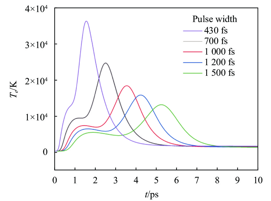
Fig. 2. Variation of electron temperature with time under laser irradiation with pulse width of 430, 700, 1000, 1200, 1500 fs and energy density of 0.35 J/cm2
Fig. 3. Variation of real and imaginary parts of dielectric constant with time under the action of pulse width of 8 ps and pulse energy density of 0.28 J/cm2
Fig. 4. Under laser irradiation with pulse width of 430 fs and 8 ps respectively, (a) change of peak carrier number density and the real part of peak dielectric constant on monocrystalline silicon surface with the change of incident laser energy density; (b) Change of peak refractive index and peak extinction coefficient on monocrystalline silicon surface with the change of incident laser energy density
Fig. 5. Changes of refractive index and extinction coefficient of silicon surface with pulse width when energy density is 0.28 J /cm2 and 0.31 J /cm2, respectively
|
Table 1. Model parameters of monocrystalline silicon

Set citation alerts for the article
Please enter your email address
© Copyright 2018-2021 | Chinese Laser Press. All Rights Reserved 沪ICP备15018463号-20