• Journal of Semiconductors
  • Vol. 44, Issue 9, 092602 (2023)
Bryan Siu Ting Tam1, Shou-Cheng Dong1,2,*, and Ching W. Tang1,2
Author Affiliations
  • 1State Key Laboratory of Advanced Displays and Optoelectronics Technologies, Department of Electronic and Computer Engineering, The Hong Kong University of Science and Technology, Clear Water Bay, Kowloon, Hong Kong, China
  • 2Institute for Advanced Study, The Hong Kong University of Science and Technology, Clear Water Bay, Kowloon, Hong Kong, China
  • show less
    DOI: 10.1088/1674-4926/44/9/092602 Cite this Article
    Bryan Siu Ting Tam, Shou-Cheng Dong, Ching W. Tang. Low-temperature conformal vacuum deposition of OLED devices using close-space sublimation[J]. Journal of Semiconductors, 2023, 44(9): 092602 Copy Citation Text show less
    (Color online) Process flow of CSS.
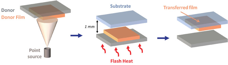
    Fig. 1. (Color online) Process flow of CSS.
    (Color online) (a) CSS setup using an electrically heated Ta foil; (b) simulated temperature distribution of the Ta foil under constant current; (c) foil temperatures under different currents with 10 s heating time; (d) the temporal profile of the evaporation rate and Ta foil temperature; (e) CSS evaporation rate of NPB films of various thicknesses from 50 to 500 nm as a function of Ta foil temperatures; (f) AFM image of a CSS-deposited NPB thin film; (g) AFM image of a VTE-deposited NPB film; (h) simulated and measured thickness profile of a CSS-deposited film from a 25 mm donor at a 1 mm gap; (i) film uniformity dependence on the donor-substrate gap and the donor dimensions; and (j) simulated thickness profile of a CSS-deposited film from a 2.5 m donor at a 20 mm gap.
    Fig. 2. (Color online) (a) CSS setup using an electrically heated Ta foil; (b) simulated temperature distribution of the Ta foil under constant current; (c) foil temperatures under different currents with 10 s heating time; (d) the temporal profile of the evaporation rate and Ta foil temperature; (e) CSS evaporation rate of NPB films of various thicknesses from 50 to 500 nm as a function of Ta foil temperatures; (f) AFM image of a CSS-deposited NPB thin film; (g) AFM image of a VTE-deposited NPB film; (h) simulated and measured thickness profile of a CSS-deposited film from a 25 mm donor at a 1 mm gap; (i) film uniformity dependence on the donor-substrate gap and the donor dimensions; and (j) simulated thickness profile of a CSS-deposited film from a 2.5 m donor at a 20 mm gap.
    (Color online) (a) CSS using a curved Ta foil; (b) schematics of CSS deposition on curved surfaces; (c) CSS-deposited NPB film on a curved stainless-steel piece; (d) fluorescent image of CSS-deposited NPB on PMMA; and (e) UV-Vis absorption spectra of CSS-deposited NPB at different locations of the PMMA substrate.
    Fig. 3. (Color online) (a) CSS using a curved Ta foil; (b) schematics of CSS deposition on curved surfaces; (c) CSS-deposited NPB film on a curved stainless-steel piece; (d) fluorescent image of CSS-deposited NPB on PMMA; and (e) UV-Vis absorption spectra of CSS-deposited NPB at different locations of the PMMA substrate.
    (Color online) (a) Radiation-heating CSS setup using a halogen bulb for device fabrication; (b) large-area radiation-heating CSS apparatus with a halogen lamp module; and (c) heating profile of the setup in (a) with a 250 W halogen bulb.
    Fig. 4. (Color online) (a) Radiation-heating CSS setup using a halogen bulb for device fabrication; (b) large-area radiation-heating CSS apparatus with a halogen lamp module; and (c) heating profile of the setup in (a) with a 250 W halogen bulb.
    (Color online) (a) The molecular structure of materials used for device fabrication; (b) device energy diagrams; (c) EQE vs. current density and (d) current density vs. voltage of blue OLEDs using CSS- and VTE-deposited NPB layers; and (e) current density vs. voltage plot of hole-only devices.
    Fig. 5. (Color online) (a) The molecular structure of materials used for device fabrication; (b) device energy diagrams; (c) EQE vs. current density and (d) current density vs. voltage of blue OLEDs using CSS- and VTE-deposited NPB layers; and (e) current density vs. voltage plot of hole-only devices.
    Current (A)Peak rate (Å/s)Tpeak (°C)
    5.40293
    5.7610142
    5.9430150
    6.30100166
    8.80489162
    Table 1. Peak temperatures and evaporation rates in CSS at different currents.
    Bryan Siu Ting Tam, Shou-Cheng Dong, Ching W. Tang. Low-temperature conformal vacuum deposition of OLED devices using close-space sublimation[J]. Journal of Semiconductors, 2023, 44(9): 092602
    Download Citation