• Photonics Research
  • Vol. 1, Issue 4, 164 (2013)
Rimlee Deb Roy, Rik Chattopadhyay, and Shyamal K. Bhadra*
Author Affiliations
  • Fiber Optics & Photonics Division, CSIR-Central Glass & Ceramic Research Institute, 196, Raja S. C. Mullick Road, Jadavpur, Kolkata 700032, India
  • show less
    DOI: 10.1364/PRJ.1.000164 Cite this Article Set citation alerts
    Rimlee Deb Roy, Rik Chattopadhyay, Shyamal K. Bhadra. Stratified composite-loaded plasmonic waveguide for sensing biofluids[J]. Photonics Research, 2013, 1(4): 164 Copy Citation Text show less
    Four-layer planar waveguide structure with embedded thin metal layer of silver (Ag).
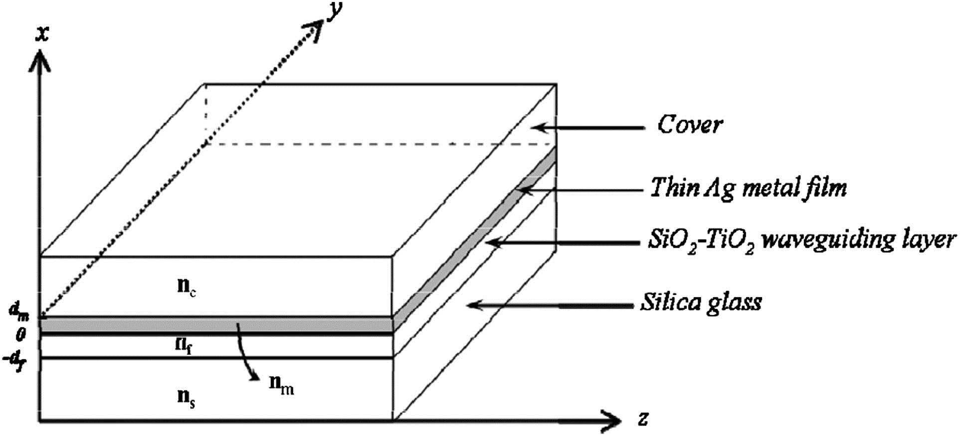
    Fig. 1. Four-layer planar waveguide structure with embedded thin metal layer of silver (Ag).
    Mode profile in transverse XY plane as obtained in (a) analytical calculation and (b) FEM using Comsol Multiphysics 4.3a. We used the values ns=1.453374, nf=1.7264, nc=1.33, df=500 nm, dm=50 nm, and λ=630 nm. RI of silver is calculated with the help of Eq. (6).
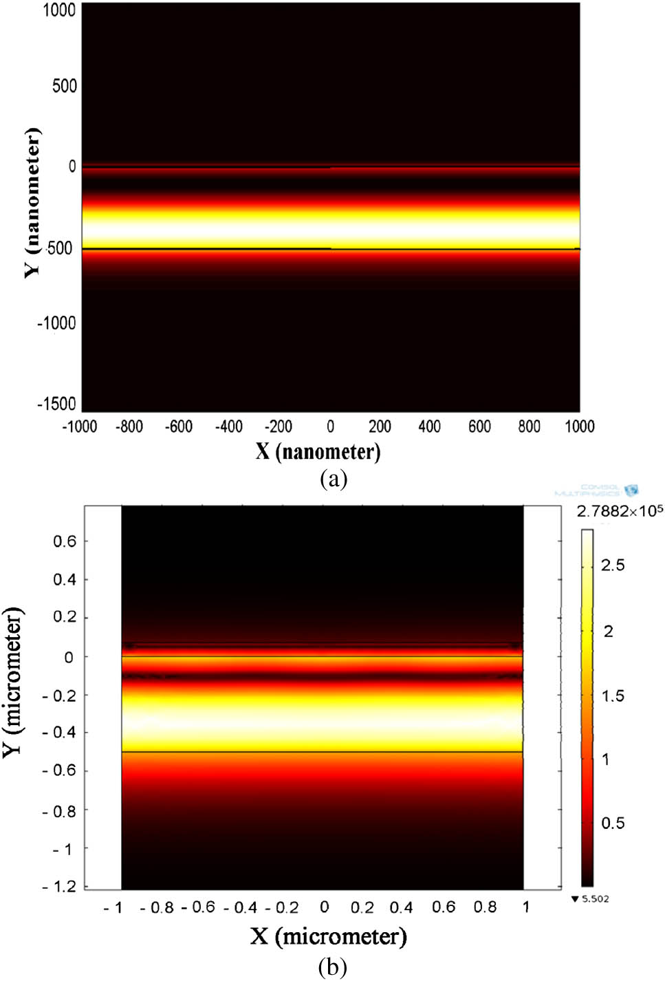
    Fig. 2. Mode profile in transverse XY plane as obtained in (a) analytical calculation and (b) FEM using Comsol Multiphysics 4.3a. We used the values ns=1.453374, nf=1.7264, nc=1.33, df=500nm, dm=50nm, and λ=630nm. RI of silver is calculated with the help of Eq. (6).
    Propagation of fundamental TM mode (Hy) at λ=630 nm. (a) XZ plane projection. (b) Three-dimensional representation from Comsol Multiphysics 4.3a. We used the values ns=1.453374, nf=1.7264, nc=1.33, df=500 nm, dm=50 nm, and λ=630 nm.
    Fig. 3. Propagation of fundamental TM mode (Hy) at λ=630nm. (a) XZ plane projection. (b) Three-dimensional representation from Comsol Multiphysics 4.3a. We used the values ns=1.453374, nf=1.7264, nc=1.33, df=500nm, dm=50nm, and λ=630nm.
    Schematic diagram of stratified medium. Gray layer indicates metal layer and white layer indicates dielectric layer.
    Fig. 4. Schematic diagram of stratified medium. Gray layer indicates metal layer and white layer indicates dielectric layer.
    Effective permittivity of the (a) real part and (b) imaginary part of the stratified layer. We took the values dsf=70 nm, dsm=30 nm, and εsd=1.42. εx, solid line; εz, broken line.
    Fig. 5. Effective permittivity of the (a) real part and (b) imaginary part of the stratified layer. We took the values dsf=70nm, dsm=30nm, and εsd=1.42. εx, solid line; εz, broken line.
    Schematic diagram of the modified plasmonic waveguide. The hashed layers are the metal layers.
    Fig. 6. Schematic diagram of the modified plasmonic waveguide. The hashed layers are the metal layers.
    Propagation of fundamental TM mode (Hy) at λ=630 nm. (a) XZ plane projection. (b) Three-dimensional representation from Comsol Multiphysics 4.3a. We used the values ns=1.453374, nf=1.7264, nc=1.33, df=500 nm, dm=50 nm, and λ=630 nm. RI of silver is calculated with the help of Eq. (6). The thickness of dielectric layer is 55 nm and the metal layer is 25 nm in the stratified layer.
    Fig. 7. Propagation of fundamental TM mode (Hy) at λ=630nm. (a) XZ plane projection. (b) Three-dimensional representation from Comsol Multiphysics 4.3a. We used the values ns=1.453374, nf=1.7264, nc=1.33, df=500nm, dm=50nm, and λ=630nm. RI of silver is calculated with the help of Eq. (6). The thickness of dielectric layer is 55 nm and the metal layer is 25 nm in the stratified layer.
    Variation of λres with nclad for different εsd (=n2 dielectric) modified waveguide with df=590 nm, dm=80 nm, nf=1.7264, and ns=1.453374.
    Fig. 8. Variation of λres with nclad for different εsd (=n2 dielectric) modified waveguide with df=590nm, dm=80nm, nf=1.7264, and ns=1.453374.
    Variation of absorption loss of the fundamental TM mode with wavelength for various analyte indices. We used the values ns=1.453374, nf=1.7264, df=650 nm, dm=73 nm, εsd=2.0164, dsf=55 nm, and dsm=28 nm.
    Fig. 9. Variation of absorption loss of the fundamental TM mode with wavelength for various analyte indices. We used the values ns=1.453374, nf=1.7264, df=650nm, dm=73nm, εsd=2.0164, dsf=55nm, and dsm=28nm.
    Comparison of absorption loss between four-layer integrated Kretschmann waveguide with bulk metal layer and loaded with stratified layer. We choose nanalyte=1.33. Both waveguides are optimized to achieve maximum absorption loss.
    Fig. 10. Comparison of absorption loss between four-layer integrated Kretschmann waveguide with bulk metal layer and loaded with stratified layer. We choose nanalyte=1.33. Both waveguides are optimized to achieve maximum absorption loss.
    Variation of absorption loss of the proposed sensor with gold used in stratified layer. We used the values ns=1.453374, nf=1.7264, df=610 nm, dm=73 nm, εsd=2.0164, dsf=60 nm, and dsm=28 nm. RI of gold is calculated with the help of Eq. (6).
    Fig. 11. Variation of absorption loss of the proposed sensor with gold used in stratified layer. We used the values ns=1.453374, nf=1.7264, df=610nm, dm=73nm, εsd=2.0164, dsf=60nm, and dsm=28nm. RI of gold is calculated with the help of Eq. (6).
    ParametersValues
    ε3.7187
    ωP(rad/s)1.396×1016
    τ0(s1)3.29×10¹⁴
    ω0(rad/s)6.496×1015
    f10.4242
    τb(s1)1.697×10¹⁶
    Table 1. Values of Different Drude–Lorentz Parameter of Ag
    Wavelength (nm)neff (Analytical)neff (Comsol)
    4501.6711533+i4.08742e31.671157+i4.089e3
    5001.6560805+i3.03639e31.656076+i3.04e3
    6301.603773+i2.092116e31.603753+i2.097e3
    7501.547821+i1.488852e31.547801+i1.49e3
    8501.504329+i1.0393e31.504556+i1.029e3
    Table 2. Values of Effective Index of Fundamental TM Mode
    Wavelength (nm)neff (Analytical)neff (Comsol)
    4501.6777598+i1.491183e31.6777806+i1.495e3
    5001.6646829+i1.83015e31.664705+i1.842e3
    6301.5975151+i7.91232e31.597124+i8.035e3
    7501.6215883+i4.3763e31.621482+i4.365e3
    8501.58031785+i3.2727e31.580277+i3.268e3
    Table 3. Values of Effective Index of Fundamental TM Mode
    Rimlee Deb Roy, Rik Chattopadhyay, Shyamal K. Bhadra. Stratified composite-loaded plasmonic waveguide for sensing biofluids[J]. Photonics Research, 2013, 1(4): 164
    Download Citation