A new integrated plasmonic waveguide sensor is reported with high sensitivity (). The integrated structure, loaded with stratified composite, makes this device robust and easy to fabricate on a chip to use as a sensor probe. The device works on the principle of resonant coupling between surface plasmon and fundamental TM mode. By selecting proper stratified structure (metal–dielectric) and core glass, one can tune the sensitivity and the range of operating wavelength.
Resonant absorption of surface plasmon is a well established technique for refractive index (RI) sensing of biofluids and chemical analytes [1–3]. In standard Kretschmann configuration, the angle of incidence corresponding to resonant absorption of surface plasmon is measured. The angle changes as the RI of the analyte changes. This configuration gives maximum sensitivity toward change in analyte RI [4–6]. The main problem of this configuration is the precise arrangement of light launching and detection. The incident light is coupled to the metal–dielectric interface through prism coupling. Sometimes high-index oil is also used in between the prism face and the sensitive layer for better coupling. It is also expected that the reflected light contains both TE and TM components. Since surface plasmon is generated only for TM modes, it is required to detect only the reflected TM light. Hence, the detection arrangement should be made selective, employing bulk optics. On the other hand, an integrated planar plasmonic waveguide structure can be fabricated with dimensions of few micrometers with significant detection sensitivity, so this type of structure can be implemented to design a sensitive probe. Like the Kretschmann configuration, the resonant coupling wavelength of the surface plasmon is measured. The resonance wavelength shifts as the index of the analyte changes.
In plasmonic waveguides, the propagating modal field through the structure gets coupled with the surface plasmon generated at the metal–dielectric interface. The coupling of the wave vector takes place through index matching between the subsequent layers, i.e., the guiding core layer and the metal or composite layer adjacent to it. In this regard, a brief mathematical description is presented in Section 2. We have modified the standard four-layer plasmonic waveguide structure, i.e., dielectric–dielectric–metal–dielectric structure, to achieve better coupling between propagating mode and surface plasmon mode. The metal layer is replaced by a metal–dielectric stratified composite layer. The composite layer shows optical anisotropy. The RIs along two perpendicular axes are different. In one direction, the layer behaves like a metal layer and along other axis it behaves as a high-index dielectric. Hence, we can align the stratified layer in such a way that it offers a negative permittivity along the transverse direction but the permittivity is positive along the direction of propagation, so a long range surface plasmon polariton (SPP) can be obtained using this stratified layer instead of bulk metal layer. A careful design of the stratified layer can shift the operating region of the sensor entirely in the visible spectrum. Hence, just by watching the color of the evanescent light, one can detect the change of analyte index.
We present an analytical model of four-layer plasmonic waveguide with bulk metal layer and stratified layer in Section 2, and later the analytical results are verified through finite element method (FEM) using Comsol Multiphysics 4.3. Then the metal layer in the surface plasmon resonance (SPR) sensor is loaded with stratified composite and the response of the structure is studied with the help of the analytical model and FEM analysis. In the last section, we present a comparison between the sensor structure loaded with bulk metal and stratified composite layer and a five-layer specialty structure with enhanced sensitivity [3].
Sign up for Photonics Research TOC. Get the latest issue of Photonics Research delivered right to you!Sign up now
2. MATHEMATICAL BACKGROUND
A. Analytical Model of Four-layer Plasmonic Waveguide
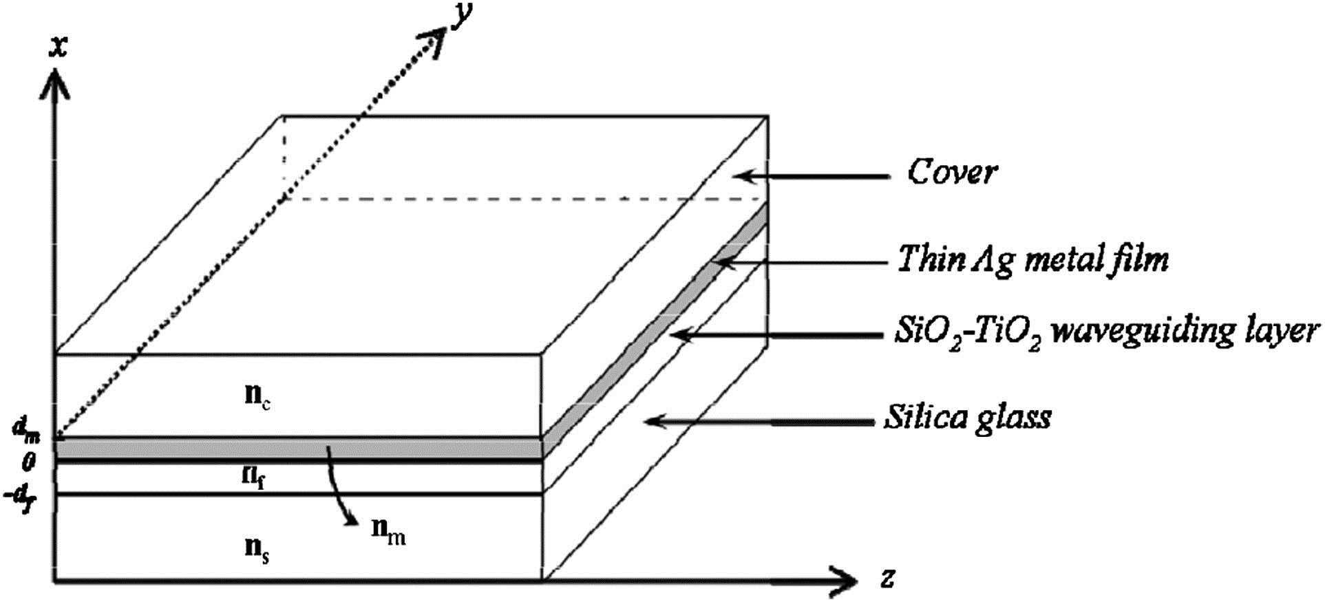
A metal-embedded, four-layer planar waveguide consists of a film of higher refractive index on a substrate of refractive index . On top of this layer, a thin layer of metal is assumed of refractive index . The fourth layer is a cover medium of refractive index as shown in Fig. 1 (schematic). Initially optimization of the all-dielectric, four-layer planar waveguide is done to obtain single-mode waveguiding [7,8]. The planar waveguide is a four-layer, all-dielectric waveguide consisting of a silica substrate on top of which a silica–titania () film of RI higher than the substrate (silica) is considered.
Figure 1.Four-layer planar waveguide structure with embedded thin metal layer of silver (Ag).
An additional thin dielectric layer of RI 1.44, which is smaller than the substrate index, and a range of values as reported elsewhere [7,8] is taken as additional guiding medium for calculation of single-mode operation at the 630 nm operating wavelength. Above this adlayer, we assume air as the cover medium. Simulation of modal propagation of such a waveguide has guided us to carry the work forward in replacing the dielectric adlayer with a thin metal film of refractive index and thickness . These thin-film waveguides are characterized by a RI variation of the form We consider the waveguide to be infinitely extended in the direction. This assumption leads to the fact that the component of the propagating electric or magnetic field is uniform, i.e., or is zero, so the propagating wave will be either transverse electric or transverse magnetic in nature. Since we are interested in studying plasmonic behavior, we shall restrict our calculation to a definite solution for the TM mode only. Therefore, we consider the input magnetic field as where , , , , , and are arbitrary constants; , , , and ; is the propagation constant of the desired mode; and is the free space wave vector at wavelength . The permittivities of the substrate, guiding layer, metal, and cover are , , , and , respectively. Now we also have the relation between the electric field component and the magnetic field component in the TM waveguide as
The appropriate boundary conditions at the interfaces are and (∵ free charge density, ).
We used the boundary condition and get the transcendental equation where the relation between and are given by the relation We assume . All other constants can be found out in terms of and . The solutions of Eqs. (4) and (5) give the propagation constants of the th order propagating mode. Now the wave vector associated with the surface plasmon at the core–metal layer interface is given as [9] Hence, maximum excitation of surface plasmon will occur at the condition . The wavelength at which this condition is satisfied is called the resonance wavelength, . We now set the values of the RIs of different layers as , , and . We choose and . The index of the metal layer is calculated through the Lorentz–Drude model given by where is the plasmon frequency of the metal, is the relaxation time, is the frequency of interest, denotes the complex number, , and the contribution from interband transitions at infinite frequency (that is, the static contribution) is . The new Lorentz term includes the Lorentz oscillator damping time , the Lorentz resonance width , and a weighting factor . The values of different parameters are given in Table 1 [10].
Parameters
Values
ε∝
3.7187
ωP(rad/s)
1.396×10¹⁶
τ0(s−1)
3.29×10⁻¹⁴
ω0(rad/s)
6.496×10¹⁵
f1
0.4242
τb(s−1)
1.697×10⁻¹⁶
Table 1. Values of Different Drude–Lorentz Parameter of Ag
We put the index values in Eqs. (4) and (5), and find out the values of at different wavelengths. Next, we analyze the structure numerically by FEM. We take the XY plane projection of the structure and run mode analysis in FEM using Comsol Multiphysics 4.3. The two results are then compared to validate the theoretical model. The results are given in Table 2. The results show a match up to the fourth decimal place.
Wavelength (nm)
neff (Analytical)
neff (Comsol)
450
1.6711533+i4.08742e−3
1.671157+i4.089e−3
500
1.6560805+i3.03639e−3
1.656076+i3.04e−3
630
1.603773+i2.092116e−3
1.603753+i2.097e−3
750
1.547821+i1.488852e−3
1.547801+i1.49e−3
850
1.504329+i1.0393e−3
1.504556+i1.029e−3
Table 2. Values of Effective Index of Fundamental TM Mode
We have optimized the structure to be single mode at 500 nm for easier detection of fundamental TM mode. The mode profiles obtained from analytical calculation and FEM analysis are shown in Fig. 2.
Figure 2.Mode profile in transverse XY plane as obtained in (a) analytical calculation and (b) FEM using Comsol Multiphysics 4.3a. We used the values , , , , , and . RI of silver is calculated with the help of Eq. (6).
We now study the propagation of the fundamental mode through the four-layer metal embedded plasmonic waveguide structure with the help of FEM simulation. We draw the XZ plane projection of the structure as shown in Fig. 1 and then set a numeric port condition at the transverse edges. A frequency domain analysis is done to obtain the and field. The propagation of the fundamental TM mode is shown in Fig. 3.
Figure 3.Propagation of fundamental TM mode () at . (a) XZ plane projection. (b) Three-dimensional representation from Comsol Multiphysics 4.3a. We used the values , , , , , and .
The three-dimensional propagation shows that the fundamental TM mode associated with a surface plasmon can propagate through the core region like a guided mode. As a result, a SPP is generated, but this SPP mode is associated with high loss (approximately at 630 nm).
B. Metal–Dielectric Stratified Medium in Waveguide and Its Advantages
We consider a stratified medium made of metal and dielectric slab. The schematic diagram of the stratified medium is shown in Fig. 4. The medium is made of periodic layers of metal film and dielectric. The thickness of each film is considered much less than the operating wavelength.
Figure 4.Schematic diagram of stratified medium. Gray layer indicates metal layer and white layer indicates dielectric layer.
The thickness of the metal layer is and that of the dielectric layer is . If the permittivities of the metal and the dielectric are and , respectively, then the permittivity of the stratified medium is given by [11–13] Equation (7) shows that a low value of can be obtained with a high value of . We designate as parallel orientation permittivity and as perpendicular orientation permittivity. We used this property of the stratified medium to obtain greater sensitivity than the four-layer plasmonic waveguide. Since the stratified medium offers an index less than 1 in parallel orientation, we replaced the metal layer shown in Fig. 1 with parallely- oriented stratified medium. Figure 5 shows the variation of and with wavelength.
Figure 5.Effective permittivity of the (a) real part and (b) imaginary part of the stratified layer. We took the values , , and . , solid line; , broken line.
The schematic diagram of the modified waveguide is shown in Fig. 6. The structure has fewer advantages than the waveguide structure shown in Fig. 1. The stratified layer behaves as the metal layer along the and axis and like the dielectric layer along the axis, so if we consider the light propagation along the axis, then the stratified layer will behave like the metal layer in the transverse plane and like the dielectric layer in the longitudinal plane. On the other hand, if we consider light propagation along the axis, then the layer will show metal-like property in the longitudinal plane and optical anisotropy in the transverse plane. In the transverse plane, it will behave like metal in one direction and like dielectric in the other perpendicular direction. This type of anisotropy cannot be achieved in the other structures mentioned earlier.
Figure 6.Schematic diagram of the modified plasmonic waveguide. The hashed layers are the metal layers.
We carried out the modal analysis and propagation characteristics of the fundamental TM mode in the structure using the analytical model and FEM-based simulation. We study the propagation characteristics in the YZ plane, i.e., we consider the light propagation along the axis. To simulate the propagation in FEM, we took the same structure as described in the previous section. Since in the present case the stratified layer is optically anisotropic, we incorporated RI anisotropy into the thin metal layer. The modal indices of fundamental TM mode at different wavelengths, as calculated from analytical model and numerically, are given in Table 3. We take and [as per Eq. (7)]. Propagation of the fundamental TM mode is shown in Fig. 7.
Figure 7.Propagation of fundamental TM mode () at . (a) XZ plane projection. (b) Three-dimensional representation from Comsol Multiphysics 4.3a. We used the values , , , , , and . RI of silver is calculated with the help of Eq. (6). The thickness of dielectric layer is 55 nm and the metal layer is 25 nm in the stratified layer.
Equation (7) shows that the RI of the stratified layer at a particular wavelength can be manipulated by changing the physical parameters. This property gives certain advantages over a bulk metal layer for designing sensors. The plasmon resonance wavelength in conventional plasmonic waveguide depends only on the waveguide parameters, i.e., the thickness and RIs of different layers. The use of stratified medium gives us one extra parameter, i.e., the RI of the dielectric used to construct the stratified layer, which plays a role to determine the resonance wavelength. The variation of the resonance wavelength () with clad layer index at different dielectric index is shown in Fig. 8.
Figure 8.Variation of with for different ( dielectric) modified waveguide with , , , and .
The optical anisotropy of the stratified layer can be utilized to construct a plasmonic waveguide which offers different permittivity along transverse and longitudinal directions. As a result, long-range SPP can be realized using the stratified layer.
3. RESULTS AND DISCUSSION
We now study the response of the waveguide shown in Fig. 6 with the help of our analytical model. We found out the spectral response of this structure for various values of the clad index. We use the analyte as clad material. Hence, the values of indices are set to the RIs of different biofluids. The resonance absorption wavelength () shifts toward the IR region as the clad index increases. The shift of with different clad layer index is shown in Fig. 9.
Figure 9.Variation of absorption loss of the fundamental TM mode with wavelength for various analyte indices. We used the values , , , , , , and .
We optimized the structure to obtain maximum sensitivity. The sensitivity of a RI sensor is normally given by the relation [14] The usual practice is to plot the against nanalyte and then calculate the slope of the line. The slope gives the average sensitivity of the system. The value of the resonance wavelength depends on the structural parameter and RIs of the constituent layers. Equation (8) shows that better sensitivity can be achieved if is large for two close values of nanalyte, so we optimized the structural parameters to achieve better sensitivity. We study the variation of sensitivity with the dielectric RI of the composite layer and also with the ratio . Based on this study, we choose the optimized value of , , and to achieve maximum sensitivity. We choose the value of , , and . It is difficult to create a stratified medium with large value, so an optimized value is chosen. We use these values in the modified structure as shown in Fig. 6, and the response of the structure for different closed values of analyte is done. The result is given in Fig. 9 which shows that, with optimized waveguide parameters, 0.001 RIU change can be sensed.
We compare the response of the modified sensor structure with conventional four-layer plasmonic waveguide. First, we optimized the conventional four-layer structure to achieve maximum sensitivity. We choose and . The absorption of the fundamental TM mode becomes highest at this structural configuration. Figure 10 shows the variation of absorption loss of fundamental TM mode with wavelength when the analyte index is set to 1.33. The result shows that the absorption is much higher at resonance condition in the modified structure. Hence, the modified structure can be used for better detection of biofluids.
Figure 10.Comparison of absorption loss between four-layer integrated Kretschmann waveguide with bulk metal layer and loaded with stratified layer. We choose . Both waveguides are optimized to achieve maximum absorption loss.
The biosensors should have a sensitive operation around RI 1.33 (aqueous region) and the operating wavelength region should be around 600–900 nm [3]. The proposed structure has operating region around 600 nm in the aqueous region. The sensor shows sensitivity of at this region. To enhance the sensitivity, we replace silver with gold. The response of the sensor with gold layer in the preferred region is better and shows sensitivity of . The result is given in Fig. 11.
Figure 11.Variation of absorption loss of the proposed sensor with gold used in stratified layer. We used the values , , , , , , and . RI of gold is calculated with the help of Eq. (6).
We compared the performance of our modified structure with a standard four-layer plasmonic waveguide with bulk metal layer structure and five-layer enhanced integrated sensor. Recent studies show that addition of a buffer layer increases the sensitivity of the plasmonic slab waveguide sensor [3]. The proposed modified plasmonic sensor is highly sensitive () in the aqueous region and can detect a change of , and the FWHM of the absorbance peak is around 20–25 nm. Though presently, new integrated plasmonic sensors are proposed which can sense RI variation as low as , our structure has some advantages over these sensors [3]. The highly sensitive integrated sensors use a bulk metal layer, so most of these sensors have a fixed wavelength region of sensing, which is dependent on the plasmon frequency of the metal. The operating region is around RI 1.44. An extra adlayer is needed to shift the region around 1.33. This additional layer decreases the sensitivity to . Since we use a stratified medium instead of a bulk metal, it is easy to shift the operating region by changing the dimensional and material parameters of the stratified layer. The stratified layer also shows maximum sensitivity around 1.33 and a comparable sensitivity of , so no adlayer is needed to shift the operating region. The FWHM of the absorption peak is around 10 nm in our proposed structure. Most of the plasmonic sensors need a polarizer at the input and output end to detect the TM modes. Since we are using a waveguide structure, this complexity may be overcome by adjusting the waveguide thickness and making the TM mode dominant in the detection process. Hence, a less complex detection arrangement may be employed. The dielectric layers in the stratified structure add an extra advantage. This dielectric can be replaced with hydrogel material, and the sensor may be converted to sense pH change [15], so our proposed sensor is useful for sensing different material properties and provides high sensitivity also. Earlier, many sensitive plasmonic structures were proposed, but they were very complicated and sometimes impossible to fabricate with available technology. The proposed structure not only gives high sensitivity but can also be fabricated with the available advanced fabrication techniques. Rapid development in the nanophotonic fabrication process made it possible to realize such sensors. The proposed stratified layer may be deposited directly onto the silica–titanium waveguide core with the help of focused ion beam (FIB) chemical vapor deposition (CVD) deposition technique. At first, the waveguide layer will be overcoated with polyvinylidene fluoride (RI value 1.42 as indicated by ASTM method D542. The low-cost polymer has a glass transition temperature of , 50%–60% crystallized, and resistance to solvents, acids, bases, and heat) and then this polymer layer could be selectively etched and silver subsequently deposited according to the design of the proposed stratified medium. This polymer has adhesive property as well, as transparent adhesive is also available of RI value 1.42, so we do not need any adhesive layer to stick the stratified layer onto the waveguide layer and the waveguide parameters will not be affected. Etching and deposition of Ag or Au are possible by FIB with precision over an appreciable surface area so that multiple photonic waveguide chips could be fabricated.
4. CONCLUSION
In this study, we present a new four-layer plasmonic sensor loaded with metal–dielectric stratified composite. The sensor shows almost comparable sensitivity () in the aqueous region to a specially designed waveguide sensor. The operating region of the sensor can be altered by changing only the thickness of the metal and dielectric layers in the stratified composite. The sensor is compact and extremely small in size, so it can be used as a sensitive probe for in situ detection of biofluids. The extremely narrow resonance absorption bandwidth will make the detection more accurate and noise free.
ACKNOWLEDGMENTS
Acknowledgment. The authors would like to acknowledge Director, CSIR-CGCRI for support and encouragement to carry out this work. Authors R. C. and R. D. R. would like to acknowledge CSIR for senior research fellowships.