Xiao Ma, Jun Zou, Wenhuan Li, Jian-Jun He, "Miniature spectrometer based on a Fourier transform spectrometer chip and a commercial photodetector array," Chin. Opt. Lett. 17, 123001 (2019)
Copy Citation Text
We demonstrate a novel type of miniature spectrometer based on a Fourier transform spectrometer (FTS) chip with a dense output array and a commercial photodetector (PD) array. The FTS chip has an output array cycle of 20 μm and consists of 51 Mach–Zehnder interferometers (MZIs), and the PD array is a commercial linear charged coupled device (CCD). An achromatic triplet lens is used to image the MZI output interferogram onto the CCD with a small aberration. Our experiment result shows that a free spectral range (FSR) from 489 nm to 584 nm and a retrieved spectral resolution of 3.5 nm at 532 nm are obtained. The achieved properties show that our spectrometer has the potential to outperform the best commercial compact one in terms of most performance indices.
It is of great importance to minimize the spectral analysis tool in order to promote its popularity in diverse applications including food safety, industrial and agricultural production, medical diagnosis, environmental protection, and so on[1–6]. To realize the miniaturization of spectrometers, an ideal choice is the planar waveguide device due to its intrinsic compactness originating from integration. Various structures have been proposed to form integrated spectrometer chips, such as microcavities, planar gratings, lattice filters, and Mach–Zehnder interferometer (MZI) arrays[7–11]. Among these configurations, the planar grating-based dispersive spectrometer chip and the MZI array-based Fourier transform spectrometer (FTS) chip are more promising due to their better overall performance and fabrication simplicity. The planar grating-based dispersive spectrometer chip usually has one input and multiple outputs, which means the input light power would be decomposed in the output edge according to the number of output channels and the spectral density distribution, while for the MZI array-based FTS chip, one input corresponds to one output; therefore, it has an intrinsic advantage of large étendue, which is quite essential for integrated chips to detect weak light in a dark environment. Another benefit of the MZI array-based FTS chip is the small temperature-dependent wavelength shift resulting from the inherent temperature compensation from the two arms of each MZI.
To integrate a waveguide spectrometer and photodetector (PD) array on a single chip is widely thought to be an ideal way to form future miniaturized spectrometers[12,13]; however, it can often be restricted by the limitation of available materials and fabrication complexity. In the foreseeable future, a separated PD array is still a more flexible and practical choice such as commercial charge coupled devices (CCDs), which are often attractive for their low cost, diversified types, and excellent performance. A drawback of the commercial PD module is that it cannot seamlessly contact a chip edge due to its surface protection layer. It may not be a problem for the dispersive spectrometer chip since light is converging in the output slab area and even if there is a gap between the PD array and the output edge, light can focus on the PD surface by simply adjusting the position of the output edge. But for the MZI array-based FTS chip, light diverging in the gap will make resolving the dense array output impossible, which is certainly necessary for the following retrieval of the original spectrum. For instance, through a 1000 μm thick protection layer, which is used in our work, the output light with a dispersion angle of 8 deg will broaden by more than 270 μm. That will cause a drastic increase of the chip size.
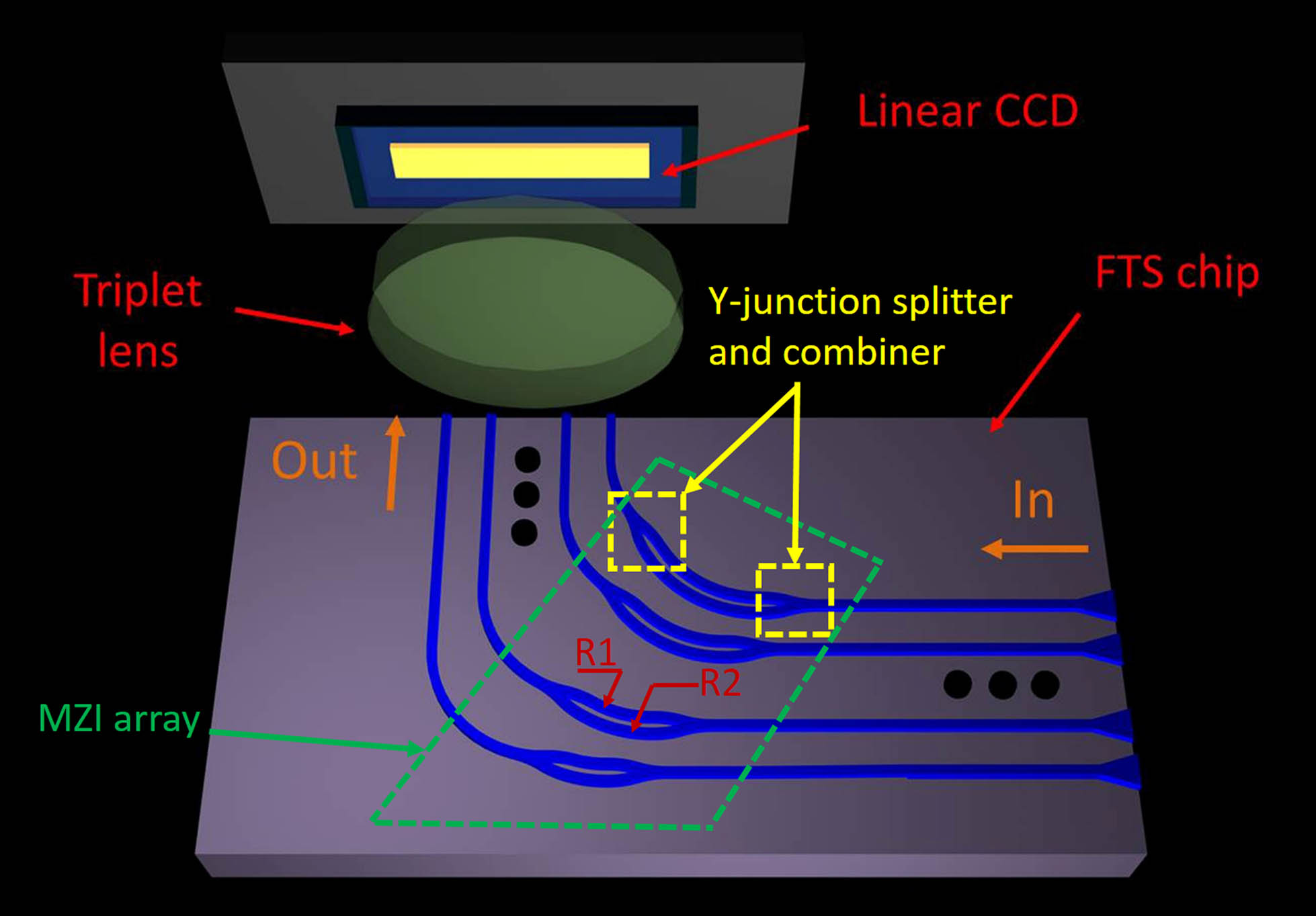
In this article, we first design, fabricate, and characterize an FTS chip operating from 489 nm to 584 nm and having an output waveguide array period of 20 μm. The FTS chip is fabricated on a low-cost silica waveguide platform and a retrieved spectral resolution of 3.5 nm at 532 nm is obtained. Then, a real spectrometer based on the fabricated FTS chip with such a dense output array and a separated commercial linear CCD is demonstrated for the first time to the best of our knowledge. To deal with the abovementioned problem of resolving a dense array output waveguide, a triplet lens is employed to image the FTS chip output onto the linear CCD with a small phase and chromatic aberration. Figure 1 shows the structure schematic of the miniaturized spectrometer.
Sign up for Chinese Optics Letters TOC. Get the latest issue of Chinese Optics Letters delivered right to you!Sign up now
Figure 1.Structure schematic of the miniaturized spectrometer. Three major parts including FTS chip, triplet lens, and linear CCD form the miniaturized spectrometer. In the FTS chip, the green box indicates the MZI array, and the yellow boxes indicate the Y-junction splitter and combiner. The two arms of each MZI have the same rotation angle but different radii as R1 and R2, leading to the OPD (optical path difference). The OPD in each MZI changes across the array along with the variation of the rotation angle.
The FTS chip we designed consists of 51 individual MZIs. Arm length difference in each MZI increases linearly by across the array. When constant input light enters into the MZI array in the input end, a modulated interferogram will present in the output end. The transmission function of each MZI can be written as where is the order number of the MZI, and is the waveguide effective refractive index of the bending arm waveguide at a specific wavenumber . represents the spectral density at a shifted wavenumber , equivalent to , in which is the Littrow number. The output interferogram can be seen as the cosine Fourier transform of the input spectrum based on the transmission function.
As shown in Fig. 1, the optical path difference (OPD) between the two arms of each MZI is caused by two bending waveguides with different radii. The parallel structure can alleviate the negative effect resulting from fabrication non-uniformity. The inverse taper in the input end is used to increase the light throughput in each MZI. To obtain a good performance in a wide spectral band, a Y-junction coupler is chosen to split and combine light to and from two arms, respectively. The directions of the input waveguide array and output waveguide array are vertical, so that the stray light can be prevented as much as possible from entering into the following photoelectric receiving system.
The cycle of the input and output waveguide array is defined to be 20 μm, in which the input and output waveguide widths are 17 μm and 3 μm, and the corresponding waveguide gaps are 3 μm and 17 μm, respectively. The refractive index difference between the core and cladding waveguide is 0.75%. The size of the bending arm channel waveguide with a bending radius of around 5000 μm is 2 μm by 1.5 μm.
The retrieved spectrum resolution and free spectral range (FSR) are denoted by[14,15]where is the total number of MZIs, is the central wavelength, and is the group refractive index of the bending waveguide. As we aim to design an FTS working from 500 nm to 600 nm, is determined to be 1 μm based on the above two equations. The average spectral resolution can be calculated as 4 nm.
Figure 2 shows the linear variation of the retrieved spectrum peak shift, with the effective refractive index change based on the theoretical simulation for a 532 nm input spectral line. The slope is 355 nm per unit index. If we consider the effective refractive index difference of between the TE and TM modes in the designed bending arms, we can know that the polarization-dependent wavelength shift would be 0.002 nm. Similarly, in consideration of the thermo-optic coefficient of per deg for silica, we can deduce that the retrieved spectrum peak will move by 0.28 nm for a temperature variation of 100 deg. Compared with the resolution of our spectrometer, neither the polarization-dependent nor the temperature-dependent wavelength shift can be neglected. This is mainly due to the small bending arm difference of 1 μm in our FTS chip.
Figure 2.Relation between the retrieved spectrum peak and the effective refractive index change.
The FTS chip we designed is fabricated on a 1.2 mm thick quartz wafer, which also functions as the lower cladding layer. A 1.5 μm thick germanium-doped silica core layer is deposited directly on the quartz by plasma enhanced vapor chemical deposition (PECVD). Then, the waveguide profile is formed through contact lithography and inductively coupled plasma (ICP) etching. Finally, an 18 μm thick upper cladding layer is developed by flame hydrolysis deposition (FHD) and thermal annealing. The overall chip size is 2 cm by 1.2 cm. Figure 3 shows a photograph of the FTS chip and the optical micrograph of its structures in part.
Figure 3.(a) Photograph of our quartz-based FTS chip next to a quarter. (b) Micrograph of adjacent splitters in two MZIs; waveguides between them are accompanying waveguides used to improve fabrication, and no light transmits in them.
The fabricated FTS chip is measured with a supercontinuum source (YSL Photonics SC-5 series), a line-width tunable filter system working between 400 nm and 810 nm, a 532 nm laser, a pair of Nufern SMJ-S405 fibers, an optical power meter, and an optical spectrum analyzer (Ando AQ6315 A).
First, we inject a wide band light into the chip and measure the entire transmission spectrum of each MZI from 460 nm to 610 nm at a sampling spacing of 0.1 nm through fiber coupling. The transformation matrix originating from transmission spectra of all the MZIs is normalized relative to the transmission spectrum of No. 0 MZI, and is presented in a two-dimensional color scaling grid array (Fig. 4) in which we find that the FSR of the FTS chip is from 489 nm to 584 nm. The difference of the measured FSR from the design value is caused by the refractive index shift of about 2.5% from the theoretically predicted value.
Figure 4.Normalized 2-D color scaling graph based on the transformation matrix resulting from the entire measured transmission spectra of all the 51 MZIs from 460 nm to 510 nm.
Second, 532 nm lasing light with a constant power is injected into each MZI, and the power vector at the output edge is obtained with our optical power meter. With the power vector , an algorithm based on pseudoinverse calculation is used to retrieve the input spectrum as , where is the pseudoinverse matrix of [16,17]. By use of the pseudoinverse method, phase and intensity errors, coupling variations over wavelength, and dispersion effects can be automatically calibrated, which is quite useful to simplify the measurement[16,17].
The original and retrieved spectra are shown in Fig. 5. The retrieved spectral peak has a bias less than the sampling resolution of 0.1 nm. The full width at half-maximum (FWHM) is 3.6 nm, which is the same as the theoretical limit at this wavelength. The residual noise alongside the spectral peak is mainly caused by the measurement setup instability. The on-chip propagation loss is measured as less than 0.5 dB/cm with the cut-off method.
Figure 5.Original and retrieved normalized spectra of the light emitted by a 532 nm laser.
After the performance of the fabricated FTS chip has been characterized and verified, it is further employed to construct a practical miniature spectrometer module by introducing a commercial linear CCD. The type of CCD we choose is Toshiba TCD1103GFG, which has 1500 image sensing elements in all. Each element is 5.5 μm in width and 64 μm in height. As we have mentioned above, the output waveguide width of each MZI in the FTS chip is 3 μm and the waveguide array period is 20 μm. If the linear CCD sensing surface could cling to the waveguide output end, the output intensity of each waveguide can be correctly obtained due to the narrow enough element width. However, the CCD has a 1 mm thick resin as the protection layer above the CCD sensing surface, which means the output light would travel freely at least 1 mm before entering into the sensing surface. With the consideration of the horizontal and vertical divergence angle of the output light as 8 deg and 10 deg, the 1/e width and height at the sensing surface would be at least 270 μm and 352 μm, respectively, based on the trigonometric functions. In that situation, we cannot resolve the output interferogram anymore.
Therefore, a triplet lens with three lenses glued together is introduced here. The radii of the four surfaces are 9.3 mm, 3.8 mm, , and ; the distances between them are 0.5 mm, 3.7 mm, and 0.5 mm; and the calculated focal length is 10.2 mm. To achieve a magnification of 1:1, the working distances between the object plane and the first surface and between the image plane and the last surface are both 18.8 mm. The spot diagrams of the triplet lens simulated by Zemax when the object height is 0 mm and 0.5 mm, are respectively presented in Fig. 6, from which we can see that the maximum geometrical radii of the light with a wavelength of 480 nm, 550 nm, and 780 nm are around 13 μm, 16 μm, and 20 μm, respectively, at a 0.5 mm object height. The maximum geometrical radii are not longer than the output waveguide array cycle; hence, by making use of the triplet lens, output light in the adjacent output waveguide will have no interference in the CCD sensing plane, theoretically.
Figure 6.Spot diagrams when (a) the object height is 0 mm and the aperture angle is 7 deg at wavelengths of 0.48 μm, 0.55 μm, and 0.78 μm; (b) the object height is 0.5 mm and the aperture angle is 7 deg at wavelengths of 0.48 μm, 0.55 μm, and 0.78 μm. The unit of the scaleplate is μm.
After mounting the FTS chip, triplet lens, and linear CCD on a mechanical fixture, a miniature spectrometer is produced, as in Fig. 7. The linear CCD converts the receiving light into a series of analog electrical signals, which are then converted to a digital signal array through an analog to digital (AD) converter. Subsequently, the digital signal array is transmitted to a computer or a smart phone through serial or wireless communication for further data processing. All the process is controlled by an Advanced RISC Machines (ARM) microcontroller unit (MCU).
Figure 7.Photograph of the mounted miniature spectrometer with the FTS chip, triplet lens, linear CCD, and a controlling electric circuit board.
We also measure the performance of the miniature spectrometer with the 532 nm laser. At this time, lasing light directly illuminates the input plane of the FTS chip without employing a fiber; the readout of the linear CCD is shown in Fig. 8. Between adjacent channels there is always a sensing element in which no light is detected, testifying the effective aberration elimination characteristic of the triplet lens. The integration time of the CCD is 41 ms when the illuminance at the input end of the chip is about 8 lx, which is fast enough for most of the applications.
Figure 8.CCD readout when 532 nm lasing light illuminates the input plane of the FTS chip. When no light enters the sensing element, the CCD readout is around 2640. The smaller the readout number is, the larger the optical power is. The red number in the figure marks the related MZI in the chip.
By summing the CCD readout of the sensing elements corresponding to each MZI, we could obtain the power vector at the output edge of the FTS chip. Multiplying with the pseudoinverse matrix , the input laser light can hereby be retrieved. From Fig. 9, we can see that the retrieved spectra through fiber coupling and CCD readout fit very well, which means that the backend system of our miniature spectrometer works very well.
Figure 9.Original and retrieved spectra of 532 nm lasing light.
Table 1 gives a side-by-side performance comparison between our miniature spectrometer and one of the most advanced and smallest commercial visible-band miniature spectrometer Hamamatsu C12666MA[18]. From the table, we can see that with a similar ratio of spectral range to resolution, our miniature spectrometer has a remarkable advantage in wavelength reproducibility and wavelength temperature dependence. Although our spectrometer is 3 times larger than the commercial counterpart in volume, it can be shrunk a lot by reducing the focal length of the triplet lens and choosing a higher refractive index difference of the waveguides. When comparing the chip-based spectrometer with the MEMS-based spectrometer, we should realize that the chip-based one is much easier for mass production with the matured semiconductor process, which means a lower cost can be achieved. Therefore, a higher potential can be expected for the chip-based spectrometer. Étendue in classical optics is equal to aperture area multiplied by solid angle (units of ), and in waveguide chips is proportional to mode field area and the square of the numerical aperture (NA). In terms of meaning, the aperture area is similar to the mode field area, and the solid angle is similar to the square of the NA. Based on Table 1, although the optical throughput of C12666MA is larger than that of our spectrometer, the impact caused by this difference is not very evident in most applications considering the surplus performance of the photodetector sensitivity. Besides, this difference is much smaller than the one between our FTS-based spectrometer chip and other types of spectrometer chip.
Parameters
Our spectrometer
C12666MA
Spectral range (nm)
489–584
340–780
Resolution (nm)
4
15
Ratio of spectral range to resolution
24
29
Size (mm)
45 × 20 × 12
20 × 13 × 10
Wavelength reproducibility (nm)
<0.1nm
<0.5nm
Wavelength temperature dependence (nm/K)
0.003
0.1
Input aperture (μm)
714 × 2
750 × 50
NA
0.04 (horizontal) 0.17 (vertical)
0.22
Table 1. Performance Comparison between Our Miniature Spectrometer and Hamamatsu C12666MA
In summary, we have designed, fabricated, and characterized an FTS chip with a dense output array on a silica waveguide platform operating from 489 nm to 584 nm. Furthermore, based on the fabricated FTS chip, we built up a novel type of miniature spectrometer system by introducing an optical detecting module including a commercial linear CCD and a triplet lens. A resolution of 3.5 nm at 532 nm was obtained through both fiber coupling and CCD readout measurement methods. For the FTS chip, it would be very convenient to extend the FSR by reducing the variation of the arm length difference between adjacent MZIs. Besides, by reducing the focal length of the triplet lens and choosing a higher refractive index difference of the waveguides, the proposed miniature spectrometer can continue to shrink in size and could be a promising spectral analysis tool in the near future due to its inherent large étendue, compactness, and low cost.
Xiao Ma, Jun Zou, Wenhuan Li, Jian-Jun He, "Miniature spectrometer based on a Fourier transform spectrometer chip and a commercial photodetector array," Chin. Opt. Lett. 17, 123001 (2019)