The finding of the robust ferroelectricity in HfO2-based thin films is fantastic from the view point of both the fundamentals and the applications. In this review article, the current research status of the future prospects for the ferroelectric HfO2-based thin films and devices are presented from fundamentals to applications. The related issues are discussed, which include: 1) The ferroelectric characteristics observed in HfO2-based films and devices associated with the factors of dopant, strain, interface, thickness, defect, fabrication condition, and more; 2) physical understanding on the observed ferroelectric behaviors by the density functional theory (DFT)-based theory calculations; 3) the characterizations of microscopic and macroscopic features by transmission electron microscopes-based and electrical properties-based techniques; 4) modeling and simulations, 5) the performance optimizations, and 6) the applications of some ferroelectric-based devices such as ferroelectric random access memory, ferroelectric-based field effect transistors, and the ferroelectric tunnel junction for the novel information processing systems.
1. Introduction
As the new ferroelectrics, hafnium oxides have attracted extensive research interests from the fundamental theories to the practical applications, due to their unexpected but robust ferroelectricity that persists even in thin films scaled down to 1 nm[1-3]. The ferroelectrics are a class of materials that have two macroscopic spontaneous polarization states, which can be reversed by the applied external electric fieldE greater than the critical electric fieldEc. In general, the spontaneous polarization states of the ferroelectrics are thermodynamically stable, but a critical temperatureTc usually exists, above which the ferroelectric turns into a paraelectric. The two critical parametersEc andTc, referred to as the coercive field and phase transition temperature respectively, are both fundamental characteristic parameters for a ferroelectric. The ferroelectricity was first discovered in the Rochelle salt in 1921[4]. Since then, the ferroelectric properties were also observed in various other material systems including KH2PO4 and alkali halide crystal families, ABO3-type perovskite oxides like BaTiO3, doped AlN like AlScN, and fluorite-type hafnia oxides like Si-doped HfO2, which have been nicely reviewed in Refs. [3,5,6]. Accompanying the discoveries of new ferroelectric materials is the boom of the ferroelectric research, ranging from the theoretical studies—the physical origins of the ferroelectricity, the correlated physical effects and models, calculation methods—to the applications of materials and devices, such as memories, sensors, actuators, energy harvesters, and neuromorphic computing cells[1-3,5-39]. Based on the different physical origins of the ferroelectricity, these various ferroelectrics have been classified into two broad types: displacive and order-disorder types[5,7-12]. For the displacive ferroelectrics like ABO3-type perovskite BaTiO3, their ferroelectricity results from thelattice phase transition—the crystal structure changes from the non-polar structure to the polar structure—associated with the condensation of a soft mode, whereas for the order-disorder type ferroelectrics like KH2PO4 (KDP) family[7] or dipole glasses[9], the ferroelectricity results from theordering phase transition of the permanent electric dipoles (induced by the cation ions or the vacancy-defects) from the disorder states at paraelectric phases to the ordered states at ferroelectric phases. The phase transition from the paraelectric to the ferroelectric usually involves the local distortions of the high-symmetry structures. In the displacive cases, the size of the local distortions is dependent on temperature across the transition but it does not change with temperature in the order-disorder cases. For both types of phase transitions, the different microscopic physical mechanisms would result in the different macroscopic physical effects on various physical fields such as temperature, stress, electric ones and more. It should be noted that the phase types of the ferroelectrics are not only associated with the crystal structure but also with the microstructures of the materials[10,11]. For instance, the behaviors associated with the order-disorder type ferroelectrics were also observed in the typical displacive type ferroelectric materials like perovskite-type PbTiO3[10].
Over more than 100 years, great advances have been achieved in the fields of ferroelectric studies and there are two key milestones, both of which are associated with the discoveries of the new class of ferroelectric materials. The first one was the discovery of perovskite ferroelectric oxides like BaTiO3, which triggered the wide research interests both in the material and device communities. Since then, the perovskite ferroelectric oxides have been in the spotlight for more than six decades until 2011. During that period, the fundamental theories regarding displacive and order-disorder types ferroelectrics/anti-ferroelectrics have been well established[7-12]. Meanwhile, the technology innovations and applications of ferroelectric materials and devices for the information storage, sensors, actuators, energy storage, and more were proposed. For details, readers are referred to Refs. [3,5,6,13,39]. The second milestone is the finding of the robust ferroelectricity in the HfO2-based materials with fluorite crystal structure, which was first reported in Si-doped thin films in 2011[1]. The implication of such a finding is profound, for both fundamentals and applications. For fundamental research, the ferroelectricity in fluorite HfO2 materials was beyond the traditional theory predictions[4]. Moreover, the robust ferroelectric characteristics demonstrated in the HfO2-based thin films could be maintained even when scaled down to less 3 nm or after more than 1012 switching cycles[2,40,41]. Meanwhile, HfO2 materials are fully compatible with CMOS technologies and have been applied in the mass production of the advanced CMOS technology nodes as high-k gate dielectrics. These fantastic characteristics of the HfO2-based ferroelectrics—robust ferroelectricity and CMOS compatibility—are exciting for the future high density integrated applications. Currently the ferroelectricity and the applications of ferroelectric HfO2-based oxides have become one of the most active research topics both in condensation state physics and microelectronics areas. The studies have covered many aspects from the fundamentals to applications, such as: 1) the process-related ferroelectric behaviors including the impacts of the dopant, strain, interface, thickness, defects, fabrication condition, and more; 2) mechanisms and theories to explain the ferroelectric behaviors; 3) the characterizations of microscopic and macroscopic features; 4) modeling and simulation, and optimization of the ferroelectric devices; and 5) the system applications. Among all, it is a particularly crucial issue to clarify the physical origins of the robust ferroelectricity in HfO2-based oxides[4]. The ferroelectricity of the HfO2-based ferroelectrics was generally attributed to the formation of polar orthorhombic phases[14]. However, various theoretical calculations have shown that the polar orthorhombic phase (O-FE) was a metastable phase for HfO2-based materials[14-17], which was not expected to produce the robust ferroelectricity in the HfO2-based thin films fabricated under the typical deposition conditions. Therefore, efforts were made to explore the key factors to stabilize the metastable O-FE such as doping, strain, interface, growth process of the thin films, and more. However, the theories on stabilizing O-FE phases are quite complicated and limited to some special cases; the conclusions sometimes are confusing and even contradictory. Such a situation implies that we may need to explore the new physical mechanisms beyond the O-FE model to understand the origin of the robust ferroelectricity in HfO2-based ferroelectric thin films and devices. Recently, we have performed DFT calculations on the monoclinic-like HfO2 films with oxygen vacancy defects (VO). The calculations indicated that oxygen vacancy defects could induce local electric dipoles in the monoclinic-like HfO2 films which resulted in the ferroelectricity when aligned in order. Such a monoclinic-like polar phase was also predicted in the oxygen vacancy ordered HfO2–δ structure[17]. Based on the new physical mechanism of the ordered VO-induced ferroelectricity, various ferroelectric/anti-ferroelectric characteristics observed in the HfO2-based ferroelectric thin films and devices such as cycling behaviors could be well explained[36]. Meanwhile, many experimental results showed the ferroelectric characteristics of HfO2-based thin films were strongly correlated with the existence of VO, which also lends support to the theory of VO-ordering induced ferroelectricity.
In this article, we will review the current research status of HfO2-based ferroelectric/anti-ferroelectric thin films from the fundamental physical mechanisms to the future system-level applications. Section I is the introduction. In Section II, we will outline the observed ferroelectric behaviors in the hafnium oxide-based materials and devices. The physical mechanisms and DFT calculations are discussed in Section III. Section IV is about the characterizations of the microscopic and macroscopic ferroelectric properties. The modeling/simulation and optimization issues of FE-based devices will be addressed in Section V and VI respectively. The system applications are presented in Section VII. The final section is the summary and future prospects on the fundamental research and technical applications.
2. Ferroelectric behaviors of HfO2-based films
The ferroelectric behaviors of HfO2-based films and devices are affected by many process-related factors. Therefore, it is essential to figure out the impact of different process conditions and the correlations between the processes to fabricate target HfO2 systems. In this section, process-related factors including doping, annealing, electrode capping, film thickness and defects (especially oxygen vacancies) will be discussed separately.
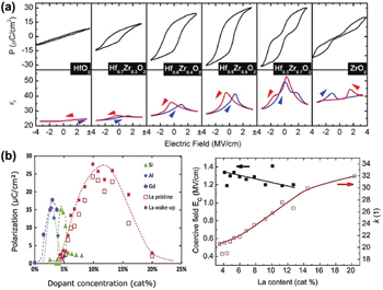
2.1. Doping effect
Ferroelectricity of HfO2 thin films was first reported in Si-doped HfO2 system by Bösckeet al. in 2011[1]. The SiO2 is considered to enhance crystallization and induce the formation of the tetragonal phase (t-phase)[42], which leads to the non-centrosymmetric orthorhombic phase (o-phase) after annealing with capping[14]. In addition to Si:HfO2[43-46], HfO2 films doped with Zr[2,20,40,47,48], Al[21,44,49], La[50-57], Y[58-61], and Gd[18,62] using prevalent atomic layer deposition (ALD) were fabricated, all of which showed the robust ferroelectricity or anti-ferroelectricity. Less commonly, ferroelectric HfO2 were prepared using other deposition methods such as sputtering, chemical solution deposition (CSD) and pulsed laser deposition (PLD). In those cases, dopants such as alkaline-earth metals (Mg, Ca, Ba)[63,64], Fe[65], N[66] were used. Depending on the dopant species, HfO2 films showed entirely different doping windows to achieve ferroelectricity, while some of the undoped HfO2 samples were found to be surprisingly ferroelectric as well[67,68]. Fabrication parameters of some of those samples are summarized inTable 1.
Table Infomation Is Not Enable
On the other hand, instead of inducing ferroelectricity, dopants may incline to stabilize t/c-phase by size modulation and oxygen vacancy (VO) formation[69,70]. For dopants radii smaller than Hf, such as Si and Al, the t-phase is more likely to form with higher doping concentration which leads to stable anti-ferroelectric-like pinched hysteresis. For larger dopants the transition to c-phase is preferred[25].
Among numerous dopants, Zr is the most widely-used dopant for ferroelectric HfO₂ because of its structural similarity to Hf and thus solid solution can be formed with a wide range of Hf : Zr atom ratios[71]. As shown inFig. 1, with increasing Zr concentration HfxZr1–xO2 system showed higher remnant polarization (Pr) which peaks at Hf : Zr atom ratio around 1 : 1. Beyond that, the anti-ferroelectricity sets in Ref. [20]. Typical 10 nm Hf0.5Zr0.5O2 (HZO) thin films whosePr are larger than 20μC/cm2 can be easily fabricated by ALD, with its coercive field (Ec) around 1 MV/cm. In recent years extremely scaled Zr:HfO2 film down to 1 nm has already been fabricated by ALD[2]. Another advantage of Zr doping is that relatively low annealing temperature around 400–600 °C is required to induce ferroelectricity, compared with other common dopants such as Si (650–1000 °C), La (650–800 °C) and Al (650–800 °C)[72], which is favorable for BEOL integration.
Figure 1.(Color online) Ferroelectric behaviors of HfO2 systems with different dopants. (a)P–E andC–E loop of Zr:HfO2 with increasing concentration.Pr is enhanced until the atom ratio of Hf : Zr reaches 1 : 1. For higher doping concentration antiferroelectricity emerges. (b) Polarization and coercive field for La:HfO2 with increasing La doping. A larger doping window of 12 mol% is observed for La compared to Si, Al and Gd. (a) is reprinted with permission from Ref. [20], copyright 2012 American Chemical Society. (b) is reprinted with permission from Ref. [53], copyright 2018 American Chemical Society.
Lanthanide elements are also considered to be strong candidates for ferroelectric HfO2 doping. Since a relatively high annealing temperature for ferroelectric La:HfO2 is required, La has been adopted to increase the crystallization temperature of HfO2 in high-k metal gate technology[73]. Theoretically, La is expected to show outstanding ferroelectric performance due to its large ionic radii and low electronegativity favoring polarPca21 space group[64,69]. Experimentally, the reported 2Pr reached 55μC/cm2 after 800 °C annealing[53]. Moreover, La tends to show a wider doping window (12 at%) than other dopants except Zr[53,64] and smaller leakage current[74].
Except for Zr and La, common elements in the semiconductor industry including Si and Al are the very first dopants that have been studied. With limited concentration window the doped HfO2 systems still show stablePr larger than 10μC/cm2. Due to the mature fabrication technology, various devices have been proposed by these common dopants[75-77]. For other dopants with larger radii such as Y, Gd and Sr, larger polarization windows (Pr > 20μC/cm2) are available by ALD, which is beneficial for memory applications.
In summary, HfO2 ferroelectricity is sensitive to doping concentration and dopant species. It should be noted that various other deposition conditions (temperature, oxygen source etc.) may also affect the performance of HfO2[72,78].
2.2. Annealing and electrode capping
Annealing temperature, pressure and atmosphere have a great impact on the formations of the crystal phase and microstructures like defects. Meanwhile, electrode capping also plays an important role in HfO2 ferroelectricity. The annealing and electrode capping effects on the ferroelectric behaviors have been investigated by using both post-metallization annealing (PMA) and post-deposition annealing (PDA) processes, where PDA refers to the annealing prior to the deposition of metal electrodes.
Several studies have investigated the formation of ferroelectric phase in HfO2 systems during the annealing, or sometimes referred to as rapid thermal process (RTP)[49,79-82]. At ambient temperature and pressure, non-centrosymmetric m-phase dominates in bulk HfO2. During annealing, t-phase or c-phase crystallites are formed at a higher temperature and then a transition to metastable orthorhombic phase takes place during the cooling process[49]. It has been calculated that the free energy barrier for the transition from t-phase to o-phase is much lower than that of transition to m-phase[83].
In most cases, the annealing temperature lies in 400–1000 °C with N2 atmosphere. Annealing under higher temperature may weaken the HfO2 ferroelectricity, which is summarized by Parket al. as the final stage in the RTP process[49]. Therefore, RTP temperature should be deliberated both to enhance the ferroelectricity and to avoid larger leakage current and lower breakdown voltage[37,80], the latter of which may be attributed to the generation of defects such as oxygen vacancies.
As mentioned above, dependent on the dopant species, different annealing temperature was adopted to stabilize the ferroelectric structures and to enhance the device reliability. For HZO systems, optimal annealing temperature lies in 400–600 °C, as shown inTable 1.Fig. 2 demonstrates that the fraction of m-phase increases with higher annealing temperature[37]. In addition, the quenching rate during the subsequent cooling process also has an impact on the ferroelectricity[84].
Figure 2.(Color online) 2Pr and o/t/m-phase fraction of (a) 5.5, (b) 10, (c) 17, (d) 25 nm HZO films annealing with different temperature.Pr is enhanced in the 400–600 °C section and the ratio of m-phase significantly increases with higher annealing temperature. Reprinted with permission from Ref. [37], copyright 2013 AIP Publishing LLC.
The deposition conditions and the annealing conditions are not independent. Low ALD temperature is needed for amorphous deposition to enhance the control over phase transition[85,86], as the suppression of the grain growth is required during the thermal process to stabilize the polar phase[37,39,85]. A higher annealing temperature is required for sputtered HfO2 film than ALD to trigger phase transition to the o-phase[87]. For PLD, the phase transition to o-phase occurs during the deposition process at high temperature and requires no follow-up annealing[72].
Nitrogen atmosphere is commonly used in ferroelectric HfO2 annealing process, as shown inTable 1. In addition to nitrogen, annealing in oxygen or forming gas atmosphere has been investigated as well[60,79,88,89]. Since oxygen vacancies are considered beneficial for FE-phase stabilization, O2 gas modifies the concentrations and distributions of oxygen vacancies and thus diminishes the ferroelectricity on the other hand[88]. Forming gas annealing is thought to contribute to the generation of oxygen vacancies due to oxygen scavenging by hydrogen[60,79]. However, hydrogen might be incorporated into HfO2 films and cause degradation to ferroelectricity[79], which requires further study on the impact of H-impurity.
Electrode capping and the strain from the electrode were considered to be beneficial for the ferroelectricity of HfO2 thin film. Hence, PMA is generally adopted to guarantee ferroelectricity in HfO2 layers. Various electrode materials were used to investigate the impacts on the ferroelectricity of HfO2 devices including TiN, Pt, TaN, W, Ti, Ir, Ni, and heavily-doped semiconductors[18,29,40,66,79,90-96], some of which are listed inTable 1. It should be noted that, besides the ferroelectricity per se, relevant aspects such as the tunneling electro-resistance (TER) and the imprint effects have to be taken into account when choosing the electrodes for memory devices[91,97], especially FTJs.
However, some PDA results showed that capping seems to not be necessary for HfO2 ferroelectricity. The ferroelectric behaviors were reported in the annealing Y-doped HfO2 films without capping[58] but the largerPr was achieved in the capped counterpart, as shown inFig. 3. A similar phenomenon was demonstrated in Al-doped HfO2 films as well[39,98]. In most cases, capped HfO2 layers possess better ferroelectricity than those without capping.
Figure 3.(a)P–V loops and (b) GIXRD patterns for Y:HfO2 undergoing 600 °C PMA and PDA process with different doping concentration. Y:HfO2 adopting PDA still shows stablePr and considerable o-phase fraction with doping concentration from 3.6 mol% to 5.2 mol%. But Y:HfO2 after PMA shows a largerPr at the same Y concentration level, which reaches 24μC/cm2 at 5.2 mol%. Reprinted with permission from Ref. [58], copyright 2011 American Institute of Physics.
Unlike conventional perovskite ferroelectric materials whose scalability are limited to ~100 nm, ferroelectric HfO2 thin films can be fabricated below 10 nm with mature CMOS technology. Although the ferroelectric o-phase was theoretically predicted to be metastable in the HfO2 system, its stability in thin films can be explained by the grain size effect, strain effect and even contribution from defects[15,27,37,48,99]. Detailed theoretical studies are reviewed in Section 3. Cheemaet al. have experimentally demonstrated that ferroelectricity could be stably maintained in sub-2 nm HZO films[2], even though the ferroelectricity was rather difficult to confirm due to a large leakage current that masked the ferroelectric switching current and the large depolarization field that suppressed the polarization[48]. Exploring the ultimate thickness of the ferroelectric HfO2 film is still ongoing. One motivation behind that is that a thinner layer with robust ferroelectricity is required for on/off current probing in ferroelectric tunnel junctions[40].
Among various deposition methods, ALD is a preferred choice for ferroelectric HfO2 films due to its excellent conformity and control over layer thickness. Plenty of experiments have demonstrated that ~10 nm is the optimal thickness for ALD-prepared ferroelectric HfO2 films, where the grain size was closely related to the deposition cycles and thickness. Parket al. examined the variations of the grain size and the remnant polarization with the HZO films thickness of 10, 17 and 25 nm and they found that the remnant polarization gradually degraded with the thicknesses, as shown inFig. 2[37]. However, for ferroelectric HfO2 films fabricated with other deposition methods, this might not be the case. The ferroelectricity withPr > 20μC/cm2 was observed in a rather thick 136 nm undoped HfO2 layer fabricated by CSD[68].
2.4. Defects and oxygen vacancies
The oxygen vacancies and interstitials are considered as the most common defects in HfO2 systems[86,100] and the concentration of oxygen vacancies in HfO2 films is highly dependent on deposition conditions. It was reported that an excessive increase of ozone dose time in the ALD process leads to a shrinking remnant polarization in ferroelectric HfO2[101-103], which was attributed to the compensation of oxygen vacancies during the subsequent deposition and annealing process. Meanwhile, in the case of lacking ozone dosage, a significant leakage current was observed, indicating a higher defect concentration[104]. However, it was also reported that both over-exposure and under-exposure to oxidation atmosphere will introduce defects[103]. Theoretically, non-polar m-phase will dominate with excessively rich oxygen vacancies[104-106]. Therefore, the appropriate dose time of oxygen is required for HfO2 films to achieve both stable ferroelectricity and good reliability.
Besides deposition and annealing atmosphere, oxygen vacancies can be modulated by capping and thus enhance ferroelectricity. For instance, Gd:HfO2 film capped by TaN electrodes shows higher remnant polarization than TiN, which was attributed to a larger amount of oxygen vacancy originating from the formation of the oxidation layer between dielectric and electrodes[18]. Similar phenomena were observed in samples with Ir/IrO2 electrodes[89,95]. Doping may also have an impact on the generation of oxygen vacancies by lowering their formation energy[86] and further discussion can be found in Section 3.
Cycling behaviors, especially wake-up and fatigue, which are important aspects of device reliability, are closely related to oxygen vacancies. A more obvious wake-up effect is observed in HfO2 films deposited by insufficient oxygen dosage, where abundant oxygen vacancies are induced[103,107]. Nevertheless, the role of oxygen vacancies in the wake-up process remains controversial. Potential mechanisms behind the wake-up effect includes modifications to local electric field, field-induced ferroelectric phase transition and domain pinning[72,86,104,105,108,109], and all of these mechanisms are associated with the generation and redistribution of oxygen vacancies. For the sake of device reliability, sufficient compensation of oxygen vacancies and the inhibition of defects is more favorable to suppress the wake-up and fatigue. Oxygen vacancies and trapping defects are also considered as contributing factors of the imprint in HfO2 films, which leads to the shift ofP–E hysteresis and further retention concern in memories. The interfacial defects near the electrode induced by the internal bias is a possible cause of this detrimental effect[105,110,111].
In summary, due to its significant impacts on the HfO2 ferroelectricity and cycling behaviors, careful considerations should be given to relevant fabrication processes in order to obtain reasonable oxygen vacancy concentration. As a side note, during the whole fabrication process other impurities also influence the quality of HfO2 film such as carbon induced by the precursor of ALD[86,112].
3. Physical mechanisms and DFT calculations
The origin of ferroelectricity in hafnia oxides needs to be understood, for the guideline of ferroelectric device design and optimization. To this aim, the first-principles calculations based on density functional theory (DFT), have been widely used for the theory investigations, due to the ability to accurately model phase stability and establish the phase diagram of hafnia. Meanwhile, the capability of independent manipulation of potential factors is advantageous to figure out the crucial factors in the emergence of ferroelectricity. In this section, we will review the progress of DFT based first-principles calculations on the ferroelectric properties of hafnia oxides.
3.1. First-principles calculations
First-principles calculations, or ab initio calculations, start directly at the level of established laws of physics without any empirical model or parameters, which is widely used in computational materials science. First-principles calculations are based on the laws of quantum mechanics and the interaction between atomic nuclei and electrons, using only the fundamental constants of physics, structure (space group), and composition of materials as the input, to solve Schrodinger equations, obtain the electronic structures, and then predict the mechanical, electronic, optical, magnetic and thermal properties. Nowadays, first-principles computations play an increasingly important role in materials science, including research on metals, oxides, 2D materials, and other complex materials. Most of first-principles calculations are based on density functional theory (DFT), in which Born-Oppenheimer approximation and Hohenberg-Kohn theorems[113] are applied to reduce computational complexity while archiving accuracy adequate for most applications. DFT calculations are often carried out within the Kohn-Sham (KS) scheme[114]. All the terms in KS equation can be evaluated exactly through a self-consistent procedure, except the exchange-correlation energy () which must be approximated. In practice the approximation for determines the quality of KS DFT calculations, so looking for accurate and generally applicable is a key issue in KS DFT. The most widely used and less time-consuming functional are the local density approximation (LDA)[114-117] and generalized gradient approximation (GGA)[118-120]. Both these two functionals could describe as the most properties of the well, including the forming energy, lattice structure and bond geometry, but fail in predictions of the band gap, due to the underestimation of the exchange interaction in functional. To solve this problem, hybrid functionals are good choices[119,121-123], which incorporate a portion of exact exchange from Hartree-Fock theory with the rest of the exchange-correlation energy from other approximations, like LDA and GGA. In conclusion, although the first-principles calculations based on DFT are independent of empirical parameters, the proper choice of the exchange-correlation energy functional is crucial for the accuracy of results.
3.2. Pressure-temperature phase diagram of HfO2
The pressure-temperature phase diagram of the bulk has been investigated experimentally by Ohtakaet al. in 2001[124], as shown inFig. 4(a). Under typical ambient conditions, the bulk crystallizes in the monoclinic phase (m phase, space group:). With increasing temperature at atmospheric pressure, the m phase transforms to a tetragonal phase (t phase, space group:) around 1973 K, and then, above 2773 K, to a cubic phase (c phase, space group:). Meanwhile, at room temperature, with increasing pressure, the stable phase of bulk transforms to the antipolar orthorhombic phase (oI phase, space group:) around 4 GPa, and then to another orthorhombic phase (oII phase, space group:) above 14.5 GPa. However, all the crystal phases are centrosymmetric, which means all of them lack a polar axis and cannot exhibit ferroelectricity. This is one of the reasons why finding ferroelectricity in-based thin films was so astonishing.
Figure 4.(Color online) (a) The experimental and (b) computed equilibrium phase diagrams of. (c) The regimes in which the free energy difference between and phases, and the equilibrium phases are small (i.e.,). (d–h) The schematic structures of m, t, oI, oII, oIII phases of respectively. (a) is reprinted with permission from Ref. [124], copyright 2023 The American Ceramic Society. (b) and (c) are reprinted with permission from Ref. [14], copyright 2014 American Physical Society.
Among the theoretical works[14,125-127] describing the existence of possible polar phases of, Huanet al. systematically searched for potential low-energy ferroelectric phases and investigated their stabilities in the pressure-temperature phase diagram[14]. First, they used a first-principles-based structure search algorithm to identify eleven low-energy phases including six nonpolar and five polar phases. All the five previously mentioned nonpolar phases observed in bulk were included. Based on the phonon band structures, free energies of dynamically stable structures among the eleven phases were computed within the harmonic approximation and a pressure-temperature phase diagram was established, shown inFig. 4(b)[14]. These results are consistent with the experimental data with a scaling factor, validating the effectiveness of this method. Then, using group theoretical symmetry reduction principles established by Shuvalov[128], two polar orthorhombic phases (oIII phase, space group:; oIV phases, space group:) were singled out that are extremely close in free energy (, where is the Boltzmann constant) to the equilibrium nonpolar phases of hafnia over a wide temperature and pressure range, illustrated inFig. 4(c). Besides, two polar rhombohedral phases (rI phase, space group:; rII phase, space group:) were proposed by Weiet al. based on their experiments and DFT calculations[129]. Of course, neither of them is the stable phase in the pressure-temperature phase diagram, while they are potential ferroelectric phases with relatively low free energy. This rII phase was predicted to be the metastable polar phase of by Barabashet al. in 2017[127]. They computed the dielectric constant but did not evaluate the actual polarization of it.
From all the results above, it suggested that ferroelectric could not be obtained by merely varying pressure and temperature, and other factors prevailing in thin films should play vital roles in the emergence of ferroelectricity, such as the size and surface effects (due to a shorter length in a dimension and the presence of electrodes), the anisotropic mechanical strains that associated with electrodes/substrates and the external electric field. The point defects including dopants and vacancies are also expected to be crucial for the ferroelectricity in thin films. Recently the intrinsic flat phonon bands of, inducing the unique scale-free ferroelectricity, have been reported[19]. This theoretical research demonstrated the importance of symmetry-distortion mode analysis. To investigate the above-mentioned effects, a comprehensive thermodynamic model of thin films must include all these energy contributions. The Gibbs free energy of this model can be defined as:
where footnote denotes the type of phase, the bulk energy including the effects of doping, vacancies, and phonon bands, the zero-point energy from vibrational modes, the hydrostatic pressure, the volume, the temperature, the entropy including vibrational and configurational entropy contribution (electronic entropy is neglected generally at room temperature because common phases of are electrical insulators with wide band gaps, around 6 eV), the surface energy, the associated surface or interface area, the electric displacement field, the electric field, the strain tensor, the stress tensor.
To investigate some specific factors, the unrelated energy contributions could be ignored, such as those energy models in works[15,99,130-132]. The thermodynamic equilibrium phase was determined by minimizing the Gibbs energy with respect to the type of phase. These factors are discussed in the following parts.
3.3. Size and surface effects on phase stability
It is known that surface and interface energy effects play an essential part in size-driven phase transformations in various nanomaterials. An example is an early research on the occurrence of the metastable tetragonal by preparing active powders with large surface areas[133]. The surface energy of t phase is smaller than that of the m phase, so with increasing surface areas, the t phase would become more stable than the m phase.
The emergence of the polar oIII phase was believed to be the structural origin of ferroelectric thin films, and was extensively used to interpret the observed behaviors in many experimental works[1,16,22,39]. Materliket al. parameterized a model by interpolating between existing data and found that the oIII phase grains were thermodynamically stable over a range of sizes[15]. This result came from the intermediate surface energy of the oIII phase, between that of the t and m phases. However, Batraet al. made a theoretical comparison of the surface energies of the major crystallographic plane of the m, t, oIII, and oIV phases showing that the surface energy is higher for all the polar phases than the m phases, except for the (001) plane[99]. Meanwhile, the (001) surface energy of the oIII phase is higher than the oIV phase, so only the polar oIV phase, instead of the polar oIII phase, could be stabilized under this mechanism in (001)-oriented thin films where the size effects dominate over the bulk energies. It should also be noted that in Batra’s energy model the surface energy is counted as free surface energy, which means the energy comes from a surface in contact with the vacuum[99]. This free surface energy model could not describe the thin films well, because the real surfaces exiting in these films are interfaces in contact with electrodes, complex grain boundaries inside the films, and interphase boundaries instead of free surfaces.
Considering the effects of interfaces with electrodes, Doganet al. established stacks to compute the energies of the interfaces between relevant phases of and typical electrode, and further built an energy model for variable-thickness films based on the interfacial energies and bulk energies[131]. The results, as depicted inFig. 5, show that the (001)-oriented m phase grains are the lowest energy configuration for all thicknesses, while the (001)-oriented oIII phase, (100)-oriented oIII phase, and (100)-oriented t phase grains are also competitive for the ultrathin films. The energy of the (100)-oriented t phase film crosses the energy of the (001)-oriented oIII phase film at a thickness of 2 unit cells (around 1nm). It means the oIII phase and m phase are dominant in thicker (above 2 unit cells) films. Chenet al. developed a multi-phase coexistence phase-field model focusing on these two phases[134]. The effects of grain boundaries were taken into account by a scale factor that can change the proportion of surface energy to the total energy of thin films. An increasing means a higher proportion of surface energy, corresponding to smaller size grains in the thin films. Due to the lower surface energy of oIII phase, compared with the m phase, the proportion of oIII phase grain increases with increasing as well as increasingly significant surface effects. This result confirms that the surface energies of grain boundaries may promote the emergence of the new polar phase in-based thin films.
Figure 5.(Color online) Thin film energies, computed via the energy model considering the interfacial energies and bulk energies, as a function of film thickness for stacks. The bulk energy of m phase is set as the zero point of bulk energies. Reprinted with permission from Ref. [131], copyright 2019 Royal Society of Chemistry.
Compared with averaging the effects of grain boundaries by a scale factor, Künnethet al. developed an energy model including the internal interface energy between the t phase and other phases and taking an experimental grain radius distribution into account[130]. They found that because the t/m phase boundary interface energy is generally higher than the t/oIII phase boundary energy, the t phase and oIII phase grain have similar energies in a wider range of grain radii, and the phase transition via kinetic means from t phase to oIII phase is more favorable than from t phase to m phase. Wuet al. found a similar result from the investigation into ferroelectric phase formation of Si-doped through nucleation[135]. Through DFT calculations, they found the t phase is the thermodynamic stable phase with the effect of dopants and surface energy at high temperatures. Meanwhile, they found the kinetic activation barrier of the phase transition from the t phase to the m phase is higher than the phase transition to the oIII phase, so when the temperature decreased the t phase grains become metastable and undergo phase transitions to the oIII phase grains. The t to oIII phase transition was directly confirmed by ab initio molecular dynamics simulation (AIMD).
Apart from the aforementioned surface effects, Leeet al. proved that the hydroxyl adsorption during the deposition process can significantly reduce the surface energy of the (112)-oriented oIII phase, leading to its emergence in ultrathin films[136].
3.4. Strain and electric field effects on phase stability
The phase stability of-based thin films is also affected by strain, which comes from the lattice constants and thermal expansion coefficient mismatch between the film and the substrate, and also from the mechanical boundaries provided by the capping electrode during the thermal annealing. Another extrinsic field, the external electric field also plays an important role in the ferroelectric-based thin films.
Considering the strain effect, we could infer that compressive strain should lower the energy difference between the polar phases (oIII, oIV, and rI phases) and the equilibrium m phase, and favor the ferroelectricity from the inverse correlation between the energies and the volumes of the various phases of[71]. This conjecture was confirmed by many first-principles calculational studies[15,131,132,137,138].
In the work of Materliket al., they found that isotropic compressive pressure could induce the phase transition from the m phase to the antipolar oI phase, consistent with the result of Huanet al.[14], and the surface effects could lower the phase transformation pressure[15]. For the anisotropic strain imposed by the substrates (which is mimiced by the constraint of a fixed surface area and zero stress in the normal direction of the film), considering that the phase transition can only happen in spatial orientations of grains with a rough match of lattice constants, they found that the (001)-oriented oIII phase with a measurable polarization in the normal direction cannot be stabilized with compressive film stress alone. Nonetheless, under the combined effects of compressive stress and electric field, the polar oIII phase could be stabilized as the equilibrium phase. Batraet al. did a similar study on the combined effects and came up with consistent results, illustrated in the computed phase diagram ofunder the influence of the electric field and in-plane stress (Fig. 6)[132].
Figure 6.(Color online) The computed phase diagram of under the influence of electric field and in-plane stress. The red, yellow, and green colors respectively mark the regions where the m, the oI, and the oIII phase are the equilibrium state. Reprinted with permission from Ref. [132], copyright 2017 American Chemical Society.
Doganet al. also investigated the trend of the energy changing of different phases with the constrained in-plane areas of grains, but instead of searching for the factors which favor the oIII phase becoming the equilibrium state, they focused on the kinetic stabilization of the polar oIII phase during thermal annealing[131]. They didn’t introduce the effect of the electric field, while they investigated the combined effects of in-plane stress, doping, and out-of-plane confinement provided by the top electrode. They found that out-of-plane confinement could suppress the t phase to m phase transformation, which is consistent with the capping effect observed in experiments[1,20,82], and doping with proper density (such as ~4% for and, and ~50% for) could favor the t phase to oIII phase transformation.
Apart from the in-plane strain of (100), (010), and (001) orientation grains studied in the aforementioned research, the (111) in-plane strain is also important and were extensively investigated because the (111)-oriented grains widely existed in epitaxial thin films[34,129]. Qiet al. found that with an in-plane shear strain, the polar oIV phase could be kinetically stabilized in (111)-oriented epitaxial films via a transition from the t phase[139]. Furthermore, the simulated x-ray diffraction (XRD) and selected area electron diffraction (SAED) of this oIV phase are consistent with the results of the experimental work[129]. Liu and Hanrahan studied the in-plane strain effects of different crystal orientations and found that both the antipolar oI phase and polar oIII phase have lower energy than the M phase with proper (111) in-plane strain and the oIII phase would become the thermodynamic stable phase with the electric field[137]. However, Zhang et al. presented that the m phase remains the most stable phase with (111) in-plane strain considering the difference in the in-plane areas of the m phase with different \lt 111 \gt orientations (such as (111) and ()), while Liu and Hanrahan did not and got the opposite result[138]. They focused on the rI phase rather than the oIII phase and found that (111) in-plane compressive stress could not stabilize the rI phase but can increase the spontaneous polarization while the rI phase could become the most stable phase under extreme film thicknesses.
To explore the physical origin of the strain effect, Delodoviciet al. studied the strain dependence of the symmetry-allowed distortions during the phase transition from the t phase to the oIII phase[140]. First, they made a symmetry-distortion mode analysis and revealed five patterns connecting the t phase and the oIII phase. Based on the Landau theory, they established the free-energy landscape described by three critical modes. Then, they analyzed the strain effect on the stability of symmetry-allowed distortion and different terms of the free-energy landscape. Finally, they found that the strong trilinear coupling among the three modes plays a vital role in stabilizing the polar oIII phase independently of the specific strain effect, while proper strain could soften the mode (i.e., the mode could become unstable with a tensile strain applied along the [100] direction).
Besides taking the energy contribution of the electric field into account, considering the forces on the ions derived from the applied electric field is also an effective method of describing the effect of the electric field and can depict the processes of structural change during phase transition. Qiet al. made phase structure optimizations with added electric field forces based on DFT calculations under finite electric fields[141]. They found that, in combination with doping effects, the t phase could transform to the polar oIII or oIV phase under an electric field and exhibit electrical hysteresis loops. Fanet al. observed similar electric-field-induced nonpolar-to-polar phase transitions and hysteresis loops in AIMD simulations[142]. They found that in-plane strain could affect the hysteresis behavior. Under the compressive in-plane strain condition, exhibits antiferroelectric behavior driven by the out-of-plane electric field, while the ferroelectric hysteresis loop emerges with tensile in-plane strain.
3.5. Point defect effects on ferroelectricity
Point defects including dopants and oxygen vacancies have been experimentally found to affect ferroelectricity in[1] thin films dramatically. The first reported ferroelectric thin film is doped with and the oxygen pressure condition during the fabrication of capacitor influences the ferroelectricity significantly[101]. Dopants in tend to form either substitutional or interstitial defects depending on atom species. First principle calculations of formation energy help to determine the dominant type of dopant defects. Oxygen vacancies are widespread in and believed to enhance ferroelectricity, and their dynamical behavior under electric field and their role as an electron trap are related to wake-up, split/merge and fatigue phenomena[31,107,143-145]. Many new mechanisms were introduced, and most of them emphasized the role of oxygen vacancies.
3.5.1. Doping effects
Dopants in tend to form either substitutional or interstitial defects depending on atom species. To determine the defect types of dopants, the relative formation energy, the differences of formation energy between substitutional and interstitial defects are calculated by first principle calculations. The relative formation energy was formulated by Duncanet al.[146]. They calculated the relative formation energy of dopants in an m phase supercell. Dopants were grouped into three groups: cation dopants, anion dopants and amphoteric dopants. Cation substitutional dopants tend to replace the Hf atom while anion dopants tend to replace the atom. The relative formation energy strongly depends on the valence of dopants. For cation dopants, the more isovalent an ion is with the species it is replacing, the more stable it was to be substitutional; the more heterovalent it is, the more stable it is to be interstitial. The of cation dopants showed strong periodicity. For anion dopants, substitutional dopants are always stable. In amphoteric dopants,,, and are the most favored. The type of dopant defects is caused by the combined effects of various factors including valency and atomic radius. Falkowskiet al. calculated the relative formation energy of various dopants using the same method as Ref. [146], and their results are shown inFig. 7[147].
Figure 7.(Color online) Formation energy of various dopants. The dopant above the red line tends to form a substitutional defect, while the dopant below the red line tends to form an interstitial defect. The red line should be located at, but Falkowskiet al. set it to 8.5 eV to compensate DFT (density functional theory) error and match experimental findings. Reprinted with permission from Ref. [147], copyright 2017 American Chemical Society.
The impacts of dopants on phase stability in doped were widely reported. Leeet al. studied doping effects on the stability of t and c phase[148]. 10 dopants including,,,, and were considered. Künnethet al. studied four-valent dopants:,,,,,, and[149]. Trivalent dopants including,, and were studied by Materliket al.[150]. Divalent dopants were reported by Materliket al. in another report[151]. Other reports focused on several specific dopants. A summary of the above reports is shown inTable 2. The strength of doping effect depends on dopant species. Batraet al. investigated 40 dopants and found that,,,,, and significantly lower the energy of the oIII phase relative to m phase[69]. Other reports found that doping effects are strong in,,,[151], and[147,152].,,, and are the most frequently studied dopants. The doping effects of,, are enhanced when oxygen vacancy forms[151]. The t phase becomes more stable than oIII phase when oxygen vacancy forms in-doped and-doped[151]. Ferroelectric oIII phase becomes more stable than nonpolar oI phase when doping concentration was large in-doped[150]. The energy decrease of t phase is large for-doped and small for- and-doped, which may explain the antiferroelectric behavior in-doped[150]. dopants can stabilize both oIII and t phase[149]. When the concentration is large, the t phase is more stable than oIII phase[149]. In the doping concentration window of 0–6.25%, the m and oI phase are more stable than ferroelectric oIII phase[147,149] in-doped. Yanget al. studied the effect of dopant ionic radius on phase stability, and found the energy of oIII and t phase relative to m phase is negatively correlated to the difference of ionic radius between dopant species and[153]. They further analyzed the phonon displacement of oIII and t phase in- and-doped. The dopant impacts phonon-mode displacement, which may be the cause of the enhancement of stability in the-doped t phase. Doping may also decrease switching barrier which leads to the lowering of the coercive field. Yanget al. calculated the switching path of- and-doped oIII phase[153].-doping reduces switching barrier significantly, therefore decreases the coercive field. However, the switching barrier of-doped remains high.
Table Infomation Is Not Enable
3.5.2. Oxygen vacancy effects
Similar to the dopants, there are also several types of oxygen defect, such as oxygen vacancy, oxygen interstitial, and oxygen Frenkel pair. Defect formation energy has a strong impact on defect species and concentrations. To investigate the formation energy of various native defects in, first-principles calculations were carried out.
Fosteret al. reported the defect formation energy of m phase and[156,157]. They found the negative-U behavior of oxygen vacancy, that two singly charged oxygen vacancies () will decay into and. The interstitial oxygen atom is more favorable than interstitial oxygen molecule in. Interstitial oxygen species and oxygen vacancies have large electron affinities, which indicates that they may serve as electron traps. These charged defects may create internal electric field, and may affect device reliability. Their study of defects in zirconia led to similar conclusions[156], due to the similar chemical properties of and caused by lanthanide contraction. Zhenget al. systematically studied the native defects in hafnia and zirconia under possible range of chemical potentials and Fermi levels[158]. The selected defect formation energy is listed inTable 3. The defect formation depended on the chemical potential and Fermi level. Under low oxygen partial pressure (reduction limit), oxygen vacancy is the most stable defect in hafnia for a wide range of Fermi levels. Under high oxygen pressure, is stable over a wide range of Fermi levels and is stable at low Fermi level. The formation energy of vacancy in is similar to that of. They also found the negative-U behavior of oxygen interstitial and vacancy in and. In most reports, fabricated thin films are non-stoichiometric and oxygen deficient[31,104], therefore, oxygen vacancy is the dominant defect in thin films. The charge state of vacancy depends on the Fermi level. To maintain charge neutrality in the bulk, Fermi level changes, which causes neutral oxygen vacancies to dominate. At interface or in thin films, charge neutrality may be violated locally[86].
Table Infomation Is Not Enable
The formation energy of oxygen vacancy can also be impacted by dopants. Zhanget al.[159] calculated the effects of metallic ion (,, and) doping on the behavior of oxygen vacancy in m phase and. Trivalent ions ( and) significantly reduce the vacancy formation energy and vacancy migration barrier. Dopant concentration also has an impact on the formation of. Zhouet al. found that was more easily to form when dopant concentration is around 3.13% in-doped[160]. Therefore, proper dopant concentration is helpful for generation.
Zhouet al. systematically investigated the effects of oxygen vacancies and dopants on the phase stability of[105]. As shown inFig. 8, with the increase of vacancy concentration, the total energies of t, oIII (marked as f inFig. 8), and oI (marked as o inFig. 8) phase decreases, though the energies of the t, oIII and oI phase are still higher than the m phase at fixed vacancy concentration. Oxygen vacancies with dopants reduce the energy of oIII phase further, compared with oxygen vacancies in undoped. Oxygen vacancies cause interface effects, and stabilize different phases under different concentrations at the interface. With no vacancy formed, the oIII phase is the most stable phase, but as the concentration of vacancies increased, m phase becomes the most stable phase, which may be relevant to the wake-up effect and fatigue effect.
Figure 8.(Color online) (a, b) Oxygen-deficient polar orthorhombic phase with different polarization orientation. (c) Total energy of the o (oI), f (oIII) and t phase relative to the m phase at different vacancy concentrations. (d) Polarization and switching barrier of the f (oIII) phase at different vacancy concentrations. Reprinted with permission from Ref. [105], copyright 2019 Elsevier B.V.
Heet al. studied the effect of charged vacancies on phase stability[161]. They calculated the energy difference of the oIII phase and m phase with different vacancy charge states at different vacancy concentrations. First-principle results showed that cannot stabilize the oIIIphase, but stabilized oIII phase when vacancy concentration is high. The energy of antipolar oI phase is lower than the oIII phase in stoichiometric. The stabilizes both phases over the m phase. Their energy difference becomes small when concentration increases. slightly increases polarization of the m and oIII phases. increases polarization of the m phase but decreases polarization of the oIII phase.
Another oxygen vacancy effect on ferroelectricity is the lowering of polarization reversal barrier. Neutral oxygen vacancy lowers the switching barrier of the oIII phase and +2 charged vacancy significantly lowers the switching barrier[162]. Leeet al. also found that the lowering of switching barrier in oxygen deficient oIII phase[163]. The oxygen deficient oIII phase has smaller lattice constants and larger remnant polarization compared with the perfect oIII phase. Zhouet al. found that spontaneous polarization of the oIII phase increases with the increase of vacancy concentration, and the switching barrier of the oIII phase first decreases and then increases with the increase of vacancy concentration, as shown inFig. 8(d)[105].
As mentioned above, the oIII phase is widely accepted as the source of spontaneous polarization in. However, theoretical calculations showed that oxygen vacancies could induce localized dipoles. Liuet al. introduced a new mechanism of ferroelectricity in based on the spontaneous polarization of the m phase with oxygen vacancies[36]. First-principle calculations showed that oxygen vacancies can induce polarization in the m phase and their migration leads to ferroelectric switching, as shown inFig. 9. Spontaneous polarization depends on the location of vacancy and varies from to. Various experimental phenomena were explained by the dynamical behavior of vacancies under the electrical field. Rushchanskiiet al. searched possible phases of oxygen deficient using the density functional theory combined with an evolutionary algorithm[17]. A fixed composition corresponding to was calculated. The total energy versus volume diagram is depicted inFig. 10. Phase M1 and M2 is two monoclinic phases with different oxygen vacancy ordering, in which M1 was the most stable phase. The perfect m phase is a centrosymmetric phase with no polarization, but the monoclinic oxygen deficient phase M1 has spontaneous polarization of, and the polarization can be switched with an energy barrier of 210. M1-O phase transition has a low switching barrier, which leads to the theoretical high mobility of M-O phase boundary in oxygen-deficient samples. The switching path of the M1 and O phases and the transition path between the M1 and O phases is depicted inFig. 11.
Figure 9.(Color online) Oxygen vacancy induced polarization and the ferroelectric switching process. Reprinted with permission from Ref. [36], copyright 2018 IEEE.
Figure 11.(Color online) Transition barrier of M–O transition (black curve, corresponds to NEB image 10–20), M1 phase switching (black curve, corresponds to NEB image 0–10) and O phase switching (red curve). Blue curve is the M–O transition in stoichiometric. Reprinted with permission from Ref. [17], copyright 2021 American Physical Society.
Recent experiment carried out by Nukalaet al. showed that oxygen vacancies in ferroelectric layer and electrodes are highly mobile under electric field, and ferroelectricity in thin films is intertwined with oxygen vacancy[34]. Therefore, theoretical study of the dynamic behavior of vacancies under the electric field can help to solve the puzzle of unexpected ferroelectricity in. Capronet al. studied the migration of oxygen vacancies in monoclinic[164]. Energy barriers of hopping between nearest-neighbor (NN) sites range between 1.84 and 3.22 eV for neutral vacancy, and significantly reduce to 0.05–1.99 eV for +2 charged vacancy, therefore charged vacancies are more mobile. The same trend was observed in the oIII phase[161]. Zhanget al. calculated the migration barrier of vacancy in m phase with various dopants.-,- and-doped and undoped were calculated, and they found that migration barrier is decreased by and dopant[159]. Zhouet al. studied the impact of vacancy concentration on the migration barrier, and found that migration barrier decreases with the increase of vacancy concentration[160].
4. Characterizations
In order to understand the ferroelectric characteristics, various experimental methods have been used to investigate the microscopic features and macroscopic behaviors of HfO2-based thin films. In this section, we will review the advances of the related characterization techniques, including the transmission electron microscope (TEM)-based techniques for the microscopic features, electrical characterization techniques for the macroscopic properties and reliability test, and the piezoresponse force microscopy for the microscopic ferroelectric domain structures.
4.1. Characterizations of nano-structural properties
With strong demands for nanotechnology innovation over the past few decades, much attention has been given to the development of the characterization methods for chemical and structural properties of nanomaterials (NMs). Among these methods, the transmission electron microscopes (TEMs) are considered the most popular technique to characterize NMs in electron microscopy. The chemical information and images of NMs at a spatial resolution of atomic dimension are provided using TEMs. In general, there are two different modes in TEMs: a fixed-beam mode (conventional TEM, CTEM) and a rastered-beam mode (STEM)[165]. Modern TEMs equipped with scanning coils are capable of both modes of operation. Both CTEM and STEM will be discussed in detail in the following section, especially focusing on their abilities to perform phase identification, crystal structure determination, as well as compositional analyses of HfO2-based ferroelectric thin films.
4.1.1. Conventional TEM techniques
The conventional TEM (CTEM) mainly refers to the basic TEM techniques i.e., electron diffraction (ED), compositional analyses and imaging techniques such as bright-field (BF), dark-field (DF) and high-resolution TEM (HRTEM)[166]. In the CTEM, the condenser lenses of the microscope are adjusted to illuminate the sample with a parallel coherent beam of electrons, usually severalμm across. A thin sample, typically less than 200 nm, is bombarded by a highly focused beam of single-energy electrons. The beam has enough energy for the electrons to be transmitted through the sample, and the transmitted or scattered electron signal is greatly magnified by a series of electromagnetic lenses[165,166]. The basic functions of CTEM are summarized inTable 4.
Table Infomation Is Not Enable
On the theoretic aspect of HRTEM imaging, based on the weak phase object approximation and an assumption of optimal focus setting, the image intensity can be directly related to the projected potential of atom columns in the crystalline specimens along the viewing direction. This provides a simple method for extracting crystal structures from HRTEM images. Nevertheless, as stressed inTable 4, it should be careful with HRTEM image interpretation. In other words, due to the strong scattering effect of matters to electrons, the weak phase object approximations only apply to very thin specimens (i.e. less than a couple of nanometers) made of light elements. Furthermore, a slight change of objective lens focus can change the feature of HRTEM images[166]. Therefore, a direct interpretation of HRTEM images as the projections of crystal structures is rarely applicable and image simulation is usually necessary to resolve atomic structures of materials from HRTEM images. In this context, there is a growing tendency to characterize the nanomaterials through the spherical aberration (Cs)-corrected STEM in recent years.
4.1.2. STEM techniques
STEM combines the principles of CTEM and scanning electron microscopy (SEM) and can be performed on either type of instrument. In the STEM, a tiny convergent electron beam is scanned over a defined area of the lamella. At each spot, the generated signal is simultaneously recorded by selected detectors, thus constructing an image. The resolution of the STEM is almost determined by the incident probe diameter on the specimen. Nowadays, a Cs-corrected STEM instrument can provide a resolution better than 0.05 nm. Furthermore, a combined use with EDS or EELS, which uses electrons transmitted through the center hole of the annular dark-field (ADF) detector, enables element analysis column by column[165,166].
In the STEM, the high angle annular dark-field (HAADF)-STEM, which selectively detects high-angle scattered electrons by annular-shaped detectors, has been actively used. The contrast of HAADF-STEM is not sensitive to small changes of defocus values and specimen thickness, thus its robust imaging characteristics allow easier interpretation of the image contrast than HRTEM methods[167,169]. However, HAADF-STEM is not capable of visualizing light element atomic columns because of its strong atomic number-dependent contrast (Z contrast). To complement HAADF-STEM, the annular bright-field (ABF)-STEM has also been developed to visualize light elements such as oxygen atomic columns inside FE-HfO2 thin films. In the ABF-STEM, electrons transmitted through specimens at each raster are detected by an annular detector inside the bright-field disk region, and thereby, light and heavy element atomic columns can be visualized as a negative image contrast irrespective of the variation of specimen thickness and defocus values[169]. The comparison of these two imaging modes of STEM is shown inTable 5.
Table Infomation Is Not Enable
It is worth noting that the integrated differential phase contrast STEM (iDPC-STEM), a new image formation method, can be also used to visualize the oxygen atomic columns. In comparison with ABF-STEM, the iDPC-STEM not only places considerably less dependence on defocus and/or thickness, but also has a higher signal-to-noise ratio[170].
4.1.3. Application of TEMs in characterization for ferroelectric HfO2 thin films
Though HfO2-based ferroelectric (FE-HfO2) thin films have been extensively studied for more than a decade, the root cause of its ferroelectricity is still a matter of debate. Perplexities and confusions arise primarily from the polymorphic nature of hafnia and also from to the challenges associated with the characterization of the mixed/complex phases in ultrathin films at small length scales[22]. In addition to some basic characterization methods such as grazing-incidence X-ray diffraction (GI-XRD) and piezoresponse force microscopy (PFM), it was increasingly obvious that the atomic resolution TEMs are becoming one of the central tools for the complete characterization of nanoscale FE-HfO2 thin films with ultrahigh spatial resolution nowadays.
The CTEM was often used to determine the cross-sectional morphology[171,172] of FE-HfO2 thin films. For instance, the layer thickness and polycrystalline nature of TiN electrodes and Hf0.5Zr0.5O2 layer in Connoret al. was clearly visualized by CTEM images[171]. Similarly, Yadavet al. employed CTEM to verify the presence of the interfacial layer in their FE-HfO2 samples and found that the device W/Hf0.5Zr0.5O2/IrOx with strong ferroelectricity contains a thinner interfacial layer than the device with W bottom electrode[172].
In fact, what makes CTEM even more powerful is its capabilities of phase identification and chemical composition analysis for polymorphic FE-HfO2 thin films[68,173-176]. For example, Bouazizet al. carried out detailed structural characterizations on the Si/TiN/(Hf,Zr)O2/TiN/Pt structures through HRTEM combined with selected area electron diffraction (SAED) and filtered Fourier transformation (FFT) patterns[173]. Another example is the study by Liet al. on Si-doped HfO2/NSTO stacks, in which cross section HRTEM images and the corresponding FFT pattern revealed that the as-grown Si-doped HfO2 films have strained fluorite structures[174].
Over the past few years, the Cs-corrected STEM methods have become a cornerstone of FE-HfO2 thin films and devices characterization owing to its ability to offer direct pictures of the samples, which could provide valuable information for optimizing the growth process to achieve targeted properties[165,166]. Grimleyet al. systematically studied interphase boundaries and single phase domains in Gd:HfO2 ferroelectric capacitors through Cs-corrected STEM[26], which were crucial to identify the ferroelectric material’s mechanical and electrical responses. As shown by HAADF-STEM images inFig. 12, a sharp O1/O2 boundary and an inter-phase O2/M1 boundary are clearly revealed. Furthermore, due to the lack of a mirror plane across the dashed axis bisecting the pattern, the position-averaged convergent beam electron diffraction (PACBED) patterns help confirm the existence ofPca21 polar phase in O1 and O2 regions. Given that HAADF-STEM images cannot directly reveal the oxygen sub-lattices, Grimleyet al. also pointed out that the schematics of the observed boundaries are approximate and represent one of several possible configurations.
Figure 12.(Color online) (a) HAADF-STEM of a pristine Gd:HfO2 grain with O and M regions separated by boundaries indicated by white arrows. (c) Magnified view of the O1/O2 boundary from (a), with (d). (b, e) Magnified regions from (a) where planes are indicated with lines and the polar direction by arrows. (f) Experiment and simulated PACBED patterns corresponding to O1 and O2 regions. Reprinted with permission from Ref. [26], copyright 2018 John Wiley & Sons, Inc.
Actually, oxygen atoms and oxygen deficiencies critically affect the ferroelectric functionality of FE-HfO2 thin films[34,163,177]. Therefore, the ABF-STEM techniques, which are capable of direct visualization of oxygen atomic columns, have become essential to the study of FE-HfO2 thin films. Chenget al. examined the crystal structures of pristine, woken-up, fatigued, and rejuvenated grains in atomic layer-deposited ferroelectric Hf0.5Zr0.5O2 thin film using the Cs-corrected ABF-STEM and HAADF-STEM techniques, as shown inFig. 13. A reversible transition between the polarPbc21 (OFE) and antipolarPbca phases (OAFE), where the crystal structures of the 180° domain wall of thePbc21 phase and the unit cell structure of thePbca phase were identical, was induced by cycling[177].
Figure 13.(Color online) The direct observation of oxygen atoms of single orthorhombic (O-) phase grain in TiN/Hf0.5Zr0.5O2 (HZO, 15 nm)/TiN device. HAADF- and ABF-STEM images of single O-phase grain (a, b) in pristine, (d, e) after wake-up process, and (f–h) after fatigue process. (c) The atomic models of thePbc21 andPbca phases along [010] direction. Reprinted with permission from REF. [177], copyright 2022 Springer Nature Limited.
Besides the imaging, another important application of STEM is analysis on the micro-area of FE-HfO2 thin films in combination with other analytical signals such as SAED, EELS and EDS, etc. For example, in a study of bulk single-crystalline Y:HfO2 deposited via a state-of-the-art laser-diode-heated floating zone technique, cell-doubling superlattice peaks in SAED patterns were observed with the existences of anti-ferroelectric polar phase (O-AP) and ferroelectric polar phase (O-FE) in the Y:HfO2 bulk single crystal samples[22].
In another work, Leeet al. investigated the effects of oxygen deficiency on the ferroelectric properties of Si:HfO2 thin films. Peak intensities in the valence EELS (VEELS) spectra and O K edge spectra consistently suggested that high-temperature annealing (HTA) films contain higher oxygen deficiency concentration than low-temperature annealing (LTA) films[163]. Furthermore, Nukalaet al. employed EDS mapping and EDS integrated spectra to reveal an accumulated effect of oxygen voltammetry in tunnel junction Co/Hf0.5Zr0.5O2(2 nm)/LSMO//STO devices[34].
The development of Cs-corrected microscopy and high-resolution spectroscopy is stepping into a golden age, it may provide a powerful platform for complete characterization of nanoscale HfO2-based thin films and devices. Except for these static structural studies, the atomic-scale visualization of structural evolution of FE-HfO2 thin films throughin situ TEMs has been one of the interesting research fields nowadays.
Meanwhile,in situ TEMs are also used to observe/monitor/record the dynamic responses and micro-structural evolution of specimen under external stimuli including heating, electricity, mechanical property, etc. To apply these external stimuli, different types of TEM holders capable of straining, lasing, heating/cooling, electricfying are available commercially or are fabricated in the laboratory[166]. The typical example regarding the study of FE-HfO2 thin films was recently set by Zhenget al. who successfully recorded the whole dynamic atomic scale structural evolution from centrosymmetric tetragonal (T-) phase to FE O-phase under electric field through HRTEM images[175]. In addition, Nukalaet al. investigated a La0.67Sr0.33MnO3/Hf0.5Zr0.5O2 capacitor interfaced with various top electrodes while performingin situ electrical bias using atomic-resolution STEM with direct oxygen imaging[34].
Forin situ experiments, the time resolution is very important to obtain experimental details. Nowadays, experiments on picosecond, or even femtosecond time scales, have been carried out by applying pulsed-electron packets, or electron pulses. Thus, it is exciting to expect more and more future studies to utilize a combination ofin situ TEMs experiments and relevant theories to further unveil the mystery of fluorite-structured ferroelectrics.
4.2. Electrical characterization
Generally, the electrical characterization is to obtain the device response to the applied voltage. This subsection presents an overview of various electrical characterizations of ferroelectric properties—both at a macroscopic and microscopic level—and of device reliability.
4.2.1. Macroscopic property characterization
In this sub subsection, the electrical characterizations of ferroelectric properties at a macroscopic level are briefly reviewed, including dynamic hysteresis measurement, DCI–V measurement,C–V measurement, first-order reversal curves (FORC) and harmonic analysis.
(1). Dynamic hysteresis measurement
Dynamic hysteresis measurement is a fundamental characterization method to confirm the existence of ferroelectricity and to extract ferroelectric properties including remnant polarizationPr, spontaneous polarizationPs, coercive field/voltageEc/Vc.
The simplest setup for hysteresis loop measurement is the Sawyer-Tower circuit[178], as shown inFig. 14, where the device under test (DUT) is connected to a reference capacitor. Only the voltage over the reference capacitor is monitored and the polarization charge can be easily calculated according to the equation, where denotes the area of the DUT. This is a charge-based method, and theoretically, arbitrary voltage waveform can be used. For more accurateP–V loop measurement, a bridge circuit with compensation for leakage current and background paraelectric current was proposed in Ref. [179] and a virtual sample grounding method was introduced in Ref. [180].
Figure 14.(Color online) (a) Sawyer-Tower circuit. (b) A circuit for transientI–V measurement. (c) A typicalP–V loop of ferroelectric capacitor. (d) A typical transient response of ferroelectric capacitor under triangle wave.
TransientI–V is another popular method forP–V measurement. Since it directly monitors both theV–t andI–t of the ferroelectric device, this method provides more details on the FE switching dynamics[181]. The occurrence of FE switching is clearly indicated by its current peaks[39,182] and the corresponding voltage is the coercive voltage, which is more precise than that extracted from theP–V loop (i.e. the horizontal intercept).
A triangular wave is applied on DUT and the current response is recorded, which has three components: leakage current, ferroelectric switching current and the background dielectric capacitance current. The leakage current is a DC component and the other two are AC components related to the voltage slope dV/dt. As the polarization charges are integrated from the FE switching current only, the non-FE components need to be removed from the measured current. Note that to remove the non-ferroelectric AC component, the dV/dt of the triangular waveform should be fixed, to ensure that the dielectric capacitance current is a constant throughout the measurement; to eliminate the effect of non-ferroelectric DC component (i.e. leakage current), larger dV/dt is usually adopted to raise the proportion of FE switching current in the measured current.
A modified method from transientI–V test called PUND (positive switching, up non-switching, negative switching, down non-switching) can also separate the non-ferroelectric components and ferroelectric switching current during the measurement[183]. The waveform of PUND is shown inFig. 15. The non-ferroelectric component— leakage current and dielectric capacitance current—is removed by subtracting the non-switching up/down part from the switching positive/negative current respectively.
Figure 15.(Color online) (a) TypicalI–V–t graph of PUND test: the applied voltage waveform (black line) and the corresponding transient current response (red line). (b) TheP–V loop of a HZO ferroelectric capacitor obtained from PUND measurement.
For FRAM and FeFET, the leakage current is unwanted and should be optimized, whereas in the ferroelectric tunneling junction (FTJ) and anti-ferroelectric tunneling junction (AFTJ), the conductance is a major property, as a large conductance difference between two polarized states (i.e. large TER) means large MW. Particularly, for multi-level FTJs[184,185] and AFTJs[186,187] memory, multiple well-separated conductance states are desired.
The conductance of the ferroelectric device is measured by DCI–V test, where the staircase or pulse sweep could be used. Note that at each voltage step, the delay time before measurement should be long enough (i.e., longer than the polarization switching time) to ensure a stable polarization state and to exclude the FE- switching AC component from the measured DC current.
(3). C–V measurement
The polymorphism of HfO₂ has long been a subject of intense research interest[18,20,82,188]. The permittivity of different phases varies greatly, ranging from ~20 to ~70[189]. Therefore, different combinations of these crystalline phases will result in different dielectric permittivity and capacitance. In turn, the phase proportions in the sample could be inferred from the measured capacitance. Therefore, the evolution of permittivity during cycling is usually interpreted as the evidence of phase transition[189,190].
InC–V measurements, a small-amplitude AC signal is superimposed on a staircase DC voltage[37,191-193]. A typical butterfly-shapedC–V curve is characteristic of the ferroelectric, whereas theC–V curve of the anti-ferroelectric is double-butterfly as shown inFig. 16. The peaks of theC–V curves are due to the contributions of domain walls during polarization switching. The permittivity is extracted using the minimum capacitance at large bias where the effect of FE switching is excluded.
Figure 16.P–E andC–E curves of (a, b) ferroelectrics and (c, d) anti-ferroelectrics
The first-order reversal curve (FORC), proposed in 2002[194], is used to determine the switching density, or so-called experimental Preisach density of the ferroelectric[194,195] films as well as the anti-ferroelectric[196,197] films.
Fig. 17 shows the waveform of FORC measurement. The DUT is first biased at positive saturation voltage. Then the applied voltage sweeps back and forth between fixed and the reversal voltage (i.e. the maximum negative voltage of each cycle, and the corresponding electric field is). The amplitude of gradually increases until it reaches the negative saturation voltage. With this, multiple FORC curves are acquired as the function of both the sweeping electric fieldE and the reversal electric field as shown inFig. 17(b) and the corresponding polarization loops as shown inFig. 17(c) can be obtained by time integration. The switching density distribution is calculated as the mixed second derivative of with respect to and. Coordinate transformation can be performed by setting,, in which is the coercive field and is the internal bias field. The final result is shown inFig. 17(d).
Figure 17.(a) First order reversal curve (FORC) test waveform, (b) FORCI–V plot, (c) FORCP–V loop, and (d) the extracted Preisach density. Reprinted with permission from Ref. [198], copyright 2015 American Chemical Society.
In addition to extracting statistical distribution of coercive field and internal bias field, FORC can also be used to distinguish between reversible and irreversible polarization contributions. Recently it has also been used to investigate the cycling behavior[199] of ferroelectric devices by monitoring the evolution of and, which has been attributed to oxygen vacancy migration and subsequently resulted in domain wall pinning/de-pinning[193].
(5). Harmonic analysis
In harmonic analysis, the polarization response to an external applied sinusoidal field is compared to the Fourier expansion of the Preisach model, both amplitudes and phases.
Morozov and Damjanovic were the first to perform this on PZT using a lock-in amplifier and up to the ninth harmonic were analyzed[200]. They found a phase jump in the third harmonic during the transition from a constricted to an open hysteresis. A similar test on Sr:HfO2 was reported in 2014[201]. Phase jumps of high order harmonics were found to indicate the redistribution of defects during wake-up or fatigue[202].
4.2.2. Reliability test
Due to their difference in device structure and hence difference in degradation mechanisms, a reliability test for the MFM capacitor and FeFET structure is discussed separately. For MFM, there are two kinds of reliability test: a retention and cycling test; for FeFET, the emphasis is placed on the interfacial layer.
(1). Reliability test for MFM structure
The polarization state of ferroelectric films can be altered over time, which is referred to as the retention characteristic. Modified from 130 nm CMOS FeRAM reliability test[203], a standard four-capacitor retention test was performed on Si-doped HfO2 capacitors, which consists of same-state (SS), new-same-state (NSS) and opposite-state (OS) retention tests[204]. The applied voltage pulse sequences are illustrated inFig. 18.
Figure 18.(Color online) 4-cap retention test. Reprinted with permission from Ref. [204], copyright 2013 IEEE.
Cycling behaviors of hafnium-based ferroelectric capacitors include wake-up, fatigue and split-up[177,182,201,204]. For the cycling test, a fixed pulse train sequence called “measure-cycling-measure” is widely adopted[201].
The cycling electrical test alone is not enough to diagnose the root cause of the cycling behaviors. Rather, comprehensive characterizations are needed. For example, Kimet al. examined the HZO film byP–V,C–V and pulse-switch test, and ascribed the cycling behavior to the formation and removal of anti-parallel domains as well as phase transition[190]. Based on the observations through STEM and FORC, Pešićet al. suggested that both oxygen vacancy induced domain pinning and phase transition are the underlying mechanisms for these cycling behaviors[104].
(2). Reliability test for FeFET
Compared with FeRAM, FeFET has poorer endurance and retention and the SiO2 interfacial layer (IL) is widely believed to be the main culprit[205-208]. Yurchuket al. investigated the role of charge trapping in reliability degradation of Si-doped HfO₂ FeFET using a single-pulse charge-trapping methodology[205,206], which monitors the threshold voltage prior and after a single pulse. They found that MW closure during cycling was predominantly determined by the LVT (low threshold voltage) shift, suggesting that the generation of fixed charges or accumulation of electrons stuck on the deep traps could be the origin of endurance degradation[205]; as for retention problem, they found that trapped charges within the ferroelectric layer compensated the polarization and reduced the memory window[206].
To investigate the relationship between interface charge trapping and FE switching in FeFET, novel measurement schemes have been proposed[209-214]. A double-sweep transientID–VG test was presented in Ref. [209], where the competition between charge trapping and polarization switching was observed in the reverse trace of the transientID–VG sweep. However, one could only tell which dominates—charge detrapping or depolarization—by the trend of transient ID. Therefore, to unravel their coupling, it is critical to quantitatively separate the charge trapping and FE switching. To this aim, a quasi-static splitC–V was modified from conventional splitC–V for FET[210], in which the gate and drain current are both recorded during the ID-VG sweep. Similarly, simultaneousP–V andI–V were proposed to separate charge-trapping and depolarization during retention[211]. Researchers from Kioxia also developed a fast charge centroid analysis scheme[214]. With this scheme, they were able to extract the time evolution of both polarization charges and trapped charges, based on which, they have proposed new mechanism for cycling degradation—cycling induced e-trapping at the FE-IL interface induces additional hole trapping during erasure[214].
Regarding the characterization of trap dynamics in FeFET, Tasneemet al. estimated the time constants as ~µs from the split PUND results and suggested that the traps are energetically close to the Si band edges and spatially located at the SiO2/HZO interface.
4.2.3. Piezoresponse force microscopy
Although the above-mentioned macroscopic electrical characterizations provide us with abundant information, observations of the domain structure and domain behaviors at nanoscale can reveal more about the polarization switching mechanism. The piezoresponse force microscopy (PFM) is a powerful tool to do this.
PFM is based on the inverse piezoelectric effect of the ferroelectric. When an AC voltage is applied on sample through the tip, the deformation of ferroelectric material causes the vibration of the cantilever, which is detected by the standard lock-in amplifier as in the traditional scanning probe microscopy (SPM). PFM can detect in-plane and out-of-plane polarization by measuring the cantilever deflection and torsion, which are called vertical PFM (VPFM) and lateral PFM (LPFM). Local strength of the effective piezoelectric coefficient is called PFM amplitude, while the phase shift between the sample and the tip is called the PFM phase. Adding DC bias meanwhile allows PFM imaging and switching local ferroelectric domains. Martinet al. examined the local ferroelectric properties of Si-doped HfO2 by single-frequency (SF) and band excitation (BE) PFM[215].
Moreover, despite of its poor time resolution, PFM can be used to observe domain dynamic behavior, such as wake-up and fatigue[61,216], imprint[110] and domain wall velocity for switch dynamics[217].
5. Modeling/Simulation
In this section, we will address the related modeling/simulation issues to ferroelectric devices (FE-based devices), which are only limited to ferroelectric random-access memory (FeRAM), ferroelectric-based field effect transistors (FeFETs), and the ferroelectric tunnel junctions (FTJs).
5.1. Polarization switching
The switching kinetics of ferroelectrics is both time- and electric field-dependent, leading to the so-called time-voltage trade-off. Therefore, the accurate polarization switching model is fundamental to the M&S of FE-based devices.
5.1.1. Preisach
The Preisach model, originated from ferromagnetics[218], was one of the most commonly used mathematical models to describe theP–E loops. The ferroelectric material was treated as a collection of parallelly-connected hysterons, each with ideally square-like hysteresis and with individual switching thresholds. The PE loop is therefore the superimposed responses of these hysterons. The distribution of the switching thresholds is defined by the Preisach function, which can be obtained experimentally or approximated with analytic functions for mathematical convenience. If the hyperbolic distribution was assumed, one can arrive at the tanh-like closed-form expression[219].
The above-mentioned classical Preisach model, though very straight-forward, is inconvenient to use. Jianget al. proposed an alternative method[220], which was computation-efficient and thus widely used[221-223]. It started with the following tanh-like expression, which provided a good fit for saturated polarization loop (or major loop).
where and are the spontaneous polarization and remanent polarization respectively, and is the coercive field. As shown inFig. 19, the unsaturated loops (or the minor loops) were obtained by linearly scaling the saturation loop accordingly[220,221]. Moreover, the history dependence of the FE hysteresis could be captured as done in Ref. [220].
Figure 19.(Color online) Minor loops are simulated by a linear scaling from the saturated polarization-voltage hysteresis loop. ↑/↓ indicates forward/reverse branch respectively. The switching dynamics are captured using a RC delay. Reprinted with permission from Ref. [221], copyright 2018 IEEE.
To cover the dynamics of polarization switching, the Preisach model is patched up with RC delay, whose time constant follows the empirical Merz law[221,224], i.e. the exponential field dependence of the switching time[225,226].
where is the input voltage and is the effective voltage that feeds into the Preisach equation. is the time constant at infinite applied field. andm are both fitting parameters. The AFE Preisach model has a similar recipe except that the major loop was constructed from two tanh functions[227,228].
5.1.2. KAI/NLS
Another widely used approach to model the ferroelectric switching was based on the Kolomogorov-Avrami growth kinetics[216], including the Kolomogorov-Avrami-Ishibashi (KAI) and nucleation-limited switching (NLS) model. The polarization reversal was divided into two stages: (1) nucleation of reversed domain; (2) forward and lateral domain growth by domain wall motion. Generally, for bulk ferroelectrics where domain growth dominated, the KAI model worked out well; whereas, for poly-crystalline thin films where the nucleation process dominated, the NLS model should be adopted instead, as it was experimentally validated with FE-HfO2 thin film[216,229-233]. Their mathematical expressions are
wheren is the effective dimension,F is the distribution function for, and is the electric field-dependent switching time expressed as:
where is the activation field, is the time constant at infinite applied field and is a fitting parameter.
The major difference between the KAI and NLS model is the switching time distribution. The former used constant (delta distribution), which was related to the macroscopic DW motion that averages system fluctuations; whereas the latter was controlled by an exponentially broad distribution of, which was related to the microscopic nucleation and thus sensitive to the local environment[234]. With the KAI model, the change in the applied voltage resulted in only shifted characteristic curves along the time-axis; while with NLS model, the slopes the characteristic curves varied with the voltage amplitude, yielding a fan-like family of curves[234].
The original NLS model is limited to polarization reversal (i.e, switching from one fully polarized state to another) under constant bias. To extend it to general polarization switching (starting from any intermediate polarization state) under arbitrary input voltage, the NLS-based Monte Carlo simulations[233,235] were proposed. The FE thin film was represented by multiple independent grains (or domains), of which each was either polarized up or down, and their activation fields were sampled from the fitting distribution. For each time interval, the switching probability of the grains was governed by the Weibull process, where a history parameter was introduced, which accounted for the FE accumulation property. The overall polarization was the ensemble average of these grains. In sum, the NLS-based MC was able to describe various FE behaviors, including the accumulation, stochasticity and variation[236].
However, the validity of the NLS model is challenged at high voltage and low temperature[237]. Weiet al. observed a transition from NLS to KAI model when then temperature was below 161 K or when the electrode size was approaching grain size[238]. Therefore, caution was suggested when dealing with these critical conditions.
On another note, the FE Monte-Carlo model can be readily modified to model AFE by considering back-switching fieldEBS[239].
Assuming that the retention loss was simply depolarization field-induced switching, the NLS model could be used to predict the retention of FE capacitors by iteratively update the remanent polarization and the depolarization field[240]. The model was confirmed to agree well with experiments at both room temperature and elevated temperature[229].
5.1.3. TDLG
The well-known Landau formalism is a phenomenological model based solely on symmetry breaking. According to the Landau theory, the free energy of ferroelectric can be expanded as polynomials of the spontaneous polarization,
where,, and are the Landau coefficients. The negative coefficient leads to the double-well energy landscape and gives the minimums values at when external filed biasE is zero. Since polarization switching was usually inhomogeneous in multi-domain (MD) ferroelectrics, Gaussian distributions of the coefficients were assumed to account for the inhomogeneity of polycrystalline thin film, similar to that of the NLS model[241,242].
If the domain wall energy is taken into account, the total energy of the system is written as follows,
where is the domain wall coupling constant, and is the electric field. With this total energy, the spatial and temporal evolution of the polarization can be described by the time-dependent Landau-Ginzburg (TDLG) equation,
where is the viscosity coefficient.
The 2D/3D phase field simulations (PFS) are achieved by solving the TDLG equation and Poisson equation in a self-consistent way[243-246], which could provide many intriguing physical insights into FE switching[247], shown asFig. 20. Sahaet al. made a detailed investigation into the accumulative polarization switching under sequential sub-Ec pulses, in which they found that the DW can potentially undergo spontaneous motion in the absence of external electric field, and that the resulting spontaneousP–Excitation/relaxation were the key mechanisms behind accumulative switching[243]. For another, instead of making presumptions about the domain number and sizes[235], the MD pattern in MFIM simulated by the PFS[244] was the result of balance between the competing energies: the depolarization energy and the DW energy. Thus, the domain number and sizes were dependent on the FE thickness and DE thickness. Likewise, the switching mode in MFIM, whether it was via nucleation-and-growth or via DW motion, was also thickness-dependent. Furthermore, the PFS could capture the stochasticity (cycle-to-cycle variation) due to different MD pattern generated in each cycle, which solely arose from the electrostatic and elastic interactions rather than thermal fluctuations[245].
Figure 20.(Color online) (a)P–E characteristics in the FE-HfO2-based MFIM structure with ferroelectric thickness of 30 nm and dielectric thickness of 5 nm. (b) Voltages, (c) electric fields, and (d) polarization charges as a function of time operated by triangular voltage waveform at frequency of 1 MHz. (e) Polarization domain patterns during the polarization switching corresponding to the stages label in (d). Reprinted with permission from Ref. [247], copyright 2021 Science China Press.
All three types of polarization switching models, in their relatively simple 1D form, could be coupled to MOSFET SPICE models and thereby used in circuit level simulations. Among all, the Preisach model was the most commonly used[221,248-251] due to its computation efficiency. The LK-based SPICE model proposed by Azizet al., used circuit-wise representation as a non-linear capacitor in series with a resistor[252,253].
5.2. FRAM cycling
Various experimental characterizations indicated that VO generation/re-distribution[31,104] and phase transition[104,189] were involved with FE cycling. It was suggested that the field-driven VO generation/distribution and the subsequent charge trapping/de-trapping would influence the ferroelectric response via the modification of local electric field or domain pinning/de-pinning as well as phase transition, which in turn changed the electric field. Pešićet al.[104] made the first attempt to qualitatively verify these complex ferroelectric and dielectric interactions in FE capacitors. They developed a framework that combined commercial TCAD and a package that model VO creation and diffusion, which could simulate theI–V andP–V characteristics of the woken-up and fatigued devices, as shown inFig. 21. However, the quantitative description of the cycling process was not available, because domain de-/pinning models and models that rigorously described the VO concentration-dependent phase transition were still lacking.
Figure 21.(Color online) Simulated wake-up of the device: (a) vacancy diffusion and (b) corresponding electric field evolution within the device with the field cycling of the FeCap in three different points in time at 4 MV/cm external applied field. (c) ResultingI–V andP–V characteristics obtained by removing the charges from the interface and changing the k-value of the grains undergoing the phase transformation. Reprinted with permission from Ref. [104], copyright 2016 John Wiley & Sons, Inc.
Liuet al.[36] proposed an alternative wake-up mechanism for FE-HfO2, in which the VO generated during cycling could possibly endow the paraelectric m-phase HfO2 with ferroelectricity. However, such acquired ferroelectricity would be lost if even number of VO take up centrosymmetric sites in the HfO2 cell, which partly explains the fatigue. Based on this mechanism, they developed a kinetic Monte Carlo (KMC) simulator which can quantitatively describe thePr evoltion by tracking the VO behaviors, as shown inFig. 22.
Figure 22.(Color online) (a) Simulated evolution of remanent polarization during the electric cycles. (b) Simulated VO distribution at different device states corresponding to the points in (a). Reprinted with permission from Ref. [36], copyright 2018 IEEE.
In addition, Chenet al. developed a phase-field polarization switching model based on the 2-D time-dependent Ginzburg–Landau (TDGL) equation coupling with Poisson’s equation that tried to explain possible mechanisms of wake-up and fatigue characteristics in the ferroelectric HfO2-based thin films[254]. In the model, the demonstrated wake-up and fatigue behaviors are related to the redistribution of nonuniform VO and its generation within the ferroelectric thin film during the cycling processes.
5.3. M&S of FeFET
The governing equations for FeFETs are the voltage balance and charge balance equations as follows[232,255].
where is the gate voltage and are the voltage drop over the FE layer and the underlying FET respectively. is the sheet carrier concentration in the MOS channel; is the polarization charge and is the trapped charges. is the electric field within the FE layer and is the permittivity of the ferroelectric.
The extra factors that came into play, specifically the trapped charges and the carriers in semiconductor, both with highly non-linear spatial, temporal and voltage dependence, making the FeFET system much more complicated than the MFM capacitor. In this section, we will cover some of the key topics in the modeling and simulation of FeFETs.
5.3.1. Mismatch between largePs and small channelQchannel
The inevitable depolarization field was both a bliss and a curse to FeFET. On one hand, the MW essentially came from the electric field effect induced by the uncompensated FE charges. On the other hand, it was the root cause of many reliability issues. In addition to the interfacial layer, the semiconductor layer also contributed greatly to the depolarization field, due to the big mismatch between typical polarization charge ~10µC/cm2 and the carrier density ~2µC/cm2. The resulting large depolarization field leaded to unexplainable large MW as well as destructive read and even write failure in the simulations[256]. There were two ways to resolve this problem. One was to force the FE to work on the minor-loop[208,244]. The other was to take the trapped charges into accounts, such as reducing the polarization charges to ~10% of thePs[256]. This was justified by the experimentally measured high interface trap density ~1014 cm–2[210], which compensated about 90% of the polarization charges[257]. In either way, the effective polarization charges were essentially reduced to 1/10 of the spontaneous polarization.
5.3.2. Interplay between polarization switching and charge trapping
The role of charge trapping is critical to FeFET performances. In this section, we focus on the dynamics in basic read/write operation. The impact of charge trapping on the FeFET reliability including retention and endurance is discussed in Section 6.2.
On one hand, the polarization charges induced larger electric field over interface layer compared to non-FE counterparts[206,258], enhancing charge injections and subsequent charge trapping. Moreover, the slow de-trapping (0.1–1 s) prohibited immediate read-after-write and hence limit high-frequency operation[208,223,257,259-261]. On the other hand, the interface tapped charges caused higher electric field over the FE layer, which enhanced polarization switching[232,262].
In spite of a few attempts with SPICE or TCAD[223,232,255,262,263], more modeling and simulation efforts are needed to validate the mechanisms suggested by experiments[210,213,214,223,257,259,264] and to deeper the understandings of the interplay between polarization switching and charge trapping.
5.3.3. relation: linear or non-linear?
The polarization chargesPFE were generally treated as sheet charges in compact models[232,263] just like the interface trapped charges and thus FE-inducedVth shift is linear dependent onPFE. However, Xianget al.’s work[255] called into question the legitimacy of simple treatment.
Based on their simulations on the 2D resistor network, they suggested that was a non-linear thresholded function ofPFE instead. Positive overallPFE would not lead to the negative unless percolation path (i.e. scattered low-conductance channel regions under the positively-switched FE domains that connect source and drain) was formed (seeFigs. 23(a) and23(b)). This work raised attention to the impacts of the spatial non-uniformity of thePFE (especially along the transverse direction). With the percolation-aware model, their simulation reproduced the ΔVTH turnaround observed in the extended measure-stress-measure (eMSM) measurement. The percolation path theory was also invoked to explain the larger average memory windows of the gate-length scaled devices[222] and the unchangedVth despited polarization loss[223].
Figure 23.(Color online) Whether percolation exists (a) or not (b) impacts theVth states. (c) Summary of percolation in FeFET. Reprinted with permission from Ref. [265], copyright 2021 IEEE.
Nonetheless, Xiang’s model neglects the carrier diffusion in semiconductors, as the 2D resistor network implicitly assumes no interactions between neighboring elements. Relatively high electron density is not confined only to the projected area of positively switched domain but expands a little bit outward[265]. Niet al.[265] re-examined the percolation-based model and concluded that channel percolation only happened when the FE domain size was larger than the carrier diffusion length.
5.3.4. Variation
Device-to-device variation is one of the key challenges for FeFET scaling as the increased variation degrades the MW of scaled devices. There were mainly three kinds of variation sources in FeFET[266]: 1) intrinsic FE variation due to reduced number of domains and FE switching stochasticity; 2) extrinsic FE variation arising from the distributions of FE parameters, namely,Ps andEc as well as FE/DE composition; 3) underlying transistor variation including random dopant fluctuation (RDF), line-edge roughness (LER), metal work function variation (WFV), interface trap (IFT) and so on. The impacts of these variation sources were evaluated with TCAD tools[222,266-268]. It was found that the variation contribution from extrinsic FE variation is much more significant than that from the underlying FET and therefore improving the uniformity of FE layer should be the primary target of variation optimization[266]. The impact of FE/DE random phase distributions on 3D NAND[269] and AND[270] FeFET architecture, and further their impacts on the in-memory computing performance was investigated by Choeet al.
5.3.5. Retention
Modeling and simulation of carrier transport in ferroelectric tunnel junction could be achieved via the following methods: (1) The Non-equilibrium Green Function (NEGF) method is a general method for modeling non-equilibrium quantum transport[280]. Moet al. studied the HfO2 MFIS-FTJ utilizing NEGF with self-consistent potential[281]. (2) WKB approximation has been widely used to investigate the tunneling transmission across the dielectric stack, and then the Tsu-Esaki model can be used to calculat the tunneling current. Based on these approaches, electrical properties of ferroelectric HfO2 based FTJ were theoretically studied[282,283]. (3) Tunneling current across the ferroelectric tunnel barriers could be calculated based on the analytical model, which was derived from the WKB approximation[284]. Different analytical formulas were used to describe the direct tunneling, Fowler-Nordheim (FN) tunneling and thermionic injection respectively. Kobayashiet al. calibrated the experimental current of ferroelectric HfO2-based MFM- and MFIS-FTJ considering the direct tunneling[285].
It was well established that the two major causes of FeFET retention loss are: 1) the depolarization field, which is responsible for the fast decay; 2) charge trapping within the gate dielectric, which dominates the long-term retention loss[271]. Due to smallerEdep/Ec ratio and smaller interface trap density, the HfO2-based FeFET outperform the perovskite counterparts[272] and extrapolated 10-year data storage was reported in many cases[208,258,273-276]. However, in the highly scaled devices, theVth became much more sensitive to the domain backswitching as there remains only a few domains. Things were even worse for multi-level memory as the intermediate state might collapse into another[277]. The NLS model, as previously shown to be able to predict the retention of FE capacitors, is a useful tool to investigate the retention performance of FeFETs, once coupled with the FET compact model. Wanget al. found that low temperature helped in preventing domain backswitching as it required longer nucleation time delay[277]. In simulations that included charge trapping, faster LVT depolarization was attributed to electron de-trapping[263,278]. Another issue during retention is imprint yet the mechanisms behind it is still under research[279].
6. Optimization of FE-based devices
In the section, we will discuss the optimization issues of the HfO2-based ferroelectric devices including ferroelectric random-access memory (FeRAM), ferroelectric-based field effect transistor (FeFET), and the ferroelectric tunnel junction (FTJ).
6.1. Optimization of FeCap and FeRAM
FeRAM possesses a similar 1T1C structure to DRAM with a ferroelectric capacitor (FeCap) connected to the drain of the transistor, which substitutes the linear capacitor storing the state “0” or “1”. Therefore, the parameters of the core FeCap are crucial for optimizing the performance of FeRAM, including remnant polarization (Pr) and coercive field (Ec). Since the two opposite states are distinguished by the polarization reversal current, charge relatedPr determines the memory window or sense margin of FeRAM, which is given by:
whereCBL refers to the bit-line parasitic capacitance andCFE is the linear capacitance of FeCap[286]. Although highPr has been achieved in metal–ferroelectric–metal (MFM) structure grown with large pad, HfO2 FeCap with stablePr has to be fabricated in the scaled integrated circuit. Meanwhile, external electric field larger thanEc is necessary for the domain reversal, which indicates a destructive readout of FeRAM. Therefore,Ec is closely related to FeRAM reliability including retention and endurance[286-288].
EnhancedPr guarantees the memory window and scalability of HfO2-based FeRAM. Most works focus on the middle of line (MOL) or back end of line (BEOL) integration of FeRAM, which adopts the mature stack structure HfO2 FeCap and has reached 130 nm node[46,289-292]. Various fabrication process may lead to differentPr in doped-HfO2 systems, which has been discussed in the previous section. Therefore, deposition and annealing conditions should be carefully designed to achieve higherPr in HfO2 FeCap. On the other hand, 3D integration provides another solution to improvePr with a small device footprint. Polakowskiet al. has demonstrated a 3D Al:HfO2 FeCap with 12 nm-thick ferroelectric layer and equivalentPr of 150μC/cm2 [293], shown asFig. 24(a). Recently an 8Gb-FeRAM array using 1X nm node DRAM technology has been fabricated by Hynix[294], with the trench capacitor insulator material replaced by HZO, shown asFig. 24(b).
Figure 24.(Color online) (a) 3D Al:HfO2 trench capacitor with trench number up to 105 and aspect ratio of 13 : 1. MeasuredPr of 12 nm Al:HfO2 with 100k trenches is 150μC/cm2. (b) 1T1C FeRAM using 1X nm node DRAM technology. At lower pulse amplitude (0.6 V) the operation of FeRAM with 5 nm HZO is possible with 2Pr of 5μC/cm2. (a) is reprinted with permission from Ref. [293], copyright 2014 IEEE. (b) is reprinted with permission from Ref. [294], copyright 2021 IEEE.
Endurance of HfO2-based FeRAM can reach 1011 cycles[289-291], which is much lower than that of DRAM (>1015 cycles) and perovskite FeRAM (>1017 cycles)[71,295]. Usually theEc of HfO2 is around 1 MV/cm, 10 times that of traditional perovskite materials, which is very close to its breakdown voltage (4–5 MV/cm) and thus limits the endurance of HfO2-based FeCap. Besides, highEc indicates a lower switching speed under the same bit-line writing voltage. Therefore, lowEc is preferred to prolong the FeRAM endurance and to enable high-speed operation. Yooet al. attempted to control the grain size of Si:HfO2 and lowerEc by different doping[296]. However, there’s a trade-off between endurance and date retention. HighEc is benefit for data retention, which is another important aspect of FeRAM reliability. Meanwhile, Penget al. demonstrated that the improved endurance performance and higher fatigue recovery capability compared to the HfZrOx (HZO) device by using HfO2-ZrO2 superlattice ferroelectric structure, where the endurance of more than 5 × 10¹² cycles was achieved[297].
As mentioned in the previous section, oxygen vacancy and other defects may have a significant impact on the device reliability issues. As fatigue and breakdown process are caused by defects generation in HfO2 thin films[104,105], compensation of those defects, especially oxygen vacancies is the central target of the selected fabrication technology, which is also benefit for wake-up free FeCaps[107]. Oxygen vacancies may also induce imprint of HfO2-based FeCap, which leads to the loss of retention because of the drift ofEc. Process optimization including sufficient oxygen dose, lowering annealing temperature, etc. has been adopted to weaken the effect of oxygen vacancy[53,103].
6.2. Optimization of FeFET
6.2.1. Memory window
Large MW is desirable to achieve a sufficiently largeIon/Ioff ratio and to mitigate the influence of variability. In particular, large MW allows for more intermediate states for multi-bit storage. Theoretically, the MW was given by the following equation[298].
where. However, the actual MWs are usually smaller than predicted[299] due to non-deal factors such as charge trapping, etc[210].
Nonetheless, increasing the ferroelectric thickness were confirmed to increase the MW[261] partly due to larger fraction of voltage drop over the FE layer. Meanwhile, increased etching difficulty as well as increased monoclinic phases came with increased[37,300] which countered the practical effect. Inserting an insulator in midst of thick FE layer could be a remedy to suppress monoclinic phases[300] and it also benefited from a largerEc[301].
According to the equation, higherPs can also help to increase MW. Besides, Ichiharaet al. suggested that most of thePs were screened by the high density interface trapped charges, leaving only a small fraction ofPs contributing to MW[257]. They hence argued thatPs increase was still effective to improve MW. For example, HZO grown on ZrO2 seed layer was improved crystalline quality and higherPs[207] and was proved to enhance FeFET MW[302].
Apart from the FE layer, optimizing the voltage drop between FE layer and the underlying FET was an alternative path and is detailed in Section 6.4. In addition, some MW optimization methods are specific to p-FeFETs and SOI-based FeFETs, which are less-studied and different from bulk n-FeFETs.
The MW of p-FeFETs and n-FeFETs was found to be asymmetric and is attributed to asymmetric charge trapping behaviors and the consequent different voltage drop over IL[303]. Based on these insights, Penget al. proposed Si-based FeFETs with thin FE and AlON IL, which by suppressing CT in n-FeFETs and increasing IL voltage drop in p-FeFET, realized almost symmetric MW in Si-based p- and n-FeFETs[304].
SOI-based FeFET suffered reduced MW at high speed because the slow carrier generation could not supply substantial minority carriers for FE switching[264,278]. In SOI-based FeFETs with gate-drain overlaps, the GIDL current was utilized to realize efficient erase operations and such effect was enhanced with larger drain bias[278].
6.2.2. Reliability
We will first briefly touch on the retention improvement and variation control. Then, we will focus on how to improve the endurance which is the most critical reliability issue for FeFET.
Minimizing the depolarization field within FE layer is critical to improving the retention of FeFETs. According to Ref. [272], this can be achieved by decreasing the capacitance of FE layer or increasing the series capacitance of the IL and Si substrate.
Complete FE switching with sufficiently large/long write pulse[233] was the most brutally simple solution to the variation problem. Other approaches as suggested by simulations called for process innovations: 1) eliminating the non-FE HfO2 grains[268]; 2) reducing the domain size (equivalently to increase the domain number)[233,236]; 3) reducing the interface trap density[222]; 4) narrowing thePs/Ec distribution[266].
The limited endurance (typically around 105) was mainly attributed to the trap generation and subsequent charge trapping in the interfacial layer (IL)[205,207,208]. Due to the largek value difference between SiO2 (~4) and HfO2 (~30), the electric field in the ILEIL is much higher than that in FE. Compared with MOSFETs, the polarization charges further increase this disproportion, enhancing charge injection and accelerating IL degradation in FeFETs[222].
Optimizing operation protocol. A workaround method was to operate in sub-loops[305] but at the cost of hazardous retention and variability. Another one exploited local heating, generated by forward current through the source/drain p–n junctions, to heal the damage at the SiON interface[306]. Periodic self-heating pulses (e.g. every 104 bipolar pulses) was shown to extend the FeFET endurance by ~1 order[307].
Tailoring the capacitive divider within the gate stack. Tailoring the capacitive divider within gate stack was another approach to reducing voltage stress on the IL, which equivalently increased MW and the larger MW was more resistant to endurance degradation. The key was to maximize the dielectric constant ratio or the area ratio[305]. Replacing the low-k SiO2 with high-k IL, such as SiON and SiNx, with a permittivity ~6 and ~8 respectively, could effectively lower theEIL[264,275]. FeFET with SiNx with endurance exceeding 1010 were successfully demonstrated[264]. Area ratio tuning is feasible in metal–ferroelectric–metal–insulator–semiconductor (MFMIS) structure. Yoonet al.[307] and Aliet al.[308] fabricated MFMIS-FETs with various which demonstrated larger MW with increased, yet the device endurance was still limited. Niet al. reported a variant MFMIS-FETs where the MFM was integrated as BEOL module. The area ratio optimization allowed the use of thick gate oxide, with low operation voltage ~1.8 V, which prevented charge trapping, thereby achieving >1010 endurance[250].
Suppress charge trapping. High pressure annealing (HPA) was reported to significantly reduce the interfacial and oxide trap density. Together with polarization enhancement and wake-up elimination, the HPA-treated FeFET also achieved endurance exceeding 1010[309]. In sub-5nm HfO2 FeFETs, hot electrons-induced hole damage close to the channel/IL was identified as the main culprit for endurance degradation[264]. In light of this, large work function gate metal was suggested as a viable option to reduce gate-side electron injection[264].
Reducing polarization charges. Although reducing effective polarization charges by controlling polarization axis alignment[305] was also a possible way to lowerEIL, there’s no experimental demonstration on FeFET for now.
6.3. Optimization of ferroelectric tunnel junction
As a two-terminal resistive memory device, ferroelectric tunnel junction (FTJ) consisted of a nanometer-thick ferroelectric layer sandwiched between top and bottom electrodes, allowing quantum tunneling through it[310]. The tunneling transmission could be effectively modulated by polarization reversal of ferroelectric leading to the ON or OFF states respectively, which could be read non-destructively.
6.3.1. Performance improvement
The tunnel electroresistance (TER) effect defined as the ON/OFF resistance ratio is an important metric for the FTJ. A larger TER ratio provides lower power consumption, better tolerance of reading errors, and even multilevel cell operation[311]. For memory sensing, the FTJ design got a enough large ON state current for faster read speed while obtaining a sufficiently large TER ratio. Several approaches were utilized to boost the ON current and TER ratio, whereas many tradeoffs needed to be managed.
Reducing the ferroelectric thickness was very effective to increase the ON current and thus reduced the operation voltage, however this approach also decreased the TER ratio. The most straightforward approach to simultaneously improved ON current and TER ratio was to increase the remnant polarization (Pr). Although the FTJs based on ultrathin perovskite ferroelectrics were achieved an excellent TER ratio due to their highPr, they suffered from the poor CMOS compatibility[312]. The HfO2 ferroelectrics are provided with good CMOS compatibility, but HfO2-based FTJs had relatively poor TER ratio, which mainly originated from the rather smallPr in reduced HfO2 film thickness[313]. To be specific, the experimentally measuredPr in 5-nm-thick HfO2 FE was about 4–17.5μC/cm2[314], while in the equal-thickness perovskites it could reach up to 31.5μC/cm2[315]. To address the poor TER ratio, the asymmetric barrier potential profiles between the top and bottom electrodes were introduced through inserting an additional insulator and/or replacing one metal electrode with a semiconductor electrode. By doing so, FTJ device structure evolved from metal-ferroelectric-metal (MFM) into metal–ferroelectric–insulator–metal (MFIM)[316] and formed metal–ferroelectric–semiconductor (MFS)[317] into metal–ferroelectric–insulator–semiconductor (MFIS)[285], which made the design space for FTJ much larger.
Note that the depolarization field (Edep) is significantly enhanced in highly asymmetric FTJs, which should be as small as possible and does not exceed coercive field (Ec) for better retention characteristics. In Ref. [318], a comprehensive modeling framework for MFIM FTJs was presented based on the Preisach model and WKB tunneling model. The tradeoff between ON current and TER ratio was revealed as a function of metal work function, band offset and permittivity of ferroelectric and insulator, and particularly a thin insulator with a high permittivity was preferable due to the mitigatedEdep. In Ref. [281], the comparison of the MFIM and MFIS FTJs was revealed based on the NEGF method, and design space of ferroelectric and insulator thickness in MFIS FTJ was provided in terms of the read current, TER ratio andEdep. In the MFIS FTJ, as semiconductor surface worked under accumulation or depletion with reversed polarization, not only the height but also the width of the barrier could be electrically modulated, leading to a greatly enhanced TER ratio. Consequently, the MFIS stack was proven to be the most potential structure for ultrathin HfO2-based FTJ.
So far, HfO2-based MFIS FTJs on n- and p-type semiconductor have been fabricated. Under similar HfO2 FE thickness (<5 nm), TER ratio in p-type device (<10) was much smaller than the n-type counterpart (<100), and the measured ON- (JON) and OFF-current (JOFF) in both n- and p-type device generally shared the same polarization polarity[2,281,319,320]. However, these behaviors could not be explained just by the depletion/accumulation for majority carriers in semiconductor electrode. To reveal their underlying conduction mechanisms, seen inFig. 25, Changet al.[282] proposed a newly multi-band tunneling model for MFIS-FTJ, accounting for electron tunneling from both the conduction band (CBE) and valence band (VBE), and hole tunneling from the valence band (VBH), which successfully explained the abovementioned issues. Particularly, VBE played an important role in determining the total current in both n- and p-type devices. It was indicated that the relative contributions of CBE, VBE and VBH strongly depend on the band diagrams which could be modulated by device structure and material property, seen inFig. 26. It was suggested that, the optimal TER for n-type device is obtained when the semiconductor surface is under depletion (accumulation) in the OFF (ON) state, whereas for p-type counterpart it was under accumulation (strong inversion) in the OFF (ON) state respectively. Based on this model, guidelines for MFIS FTJ optimization by band structure engineering is provided, and co-design of the metal and semiconductor electrodes, including the metal work function, doping type and concentration was achieved[283].
Figure 25.(Color online) (a) Band diagram of metal/FE-HfO2/SiO2/Si FTJs, where the total tunneling current consists of tunneling current from the CBE (JCBE), VBE (JVBE) and VBH (JVBH). (b) and (c) Comparison of the calculated and measured read current of FTJ based on MFIS(n+) and MFIS(p+). (d) and (e) Corresponding contributions ofJCBE,JVBE and JVBH to the total current. Reprinted with permission from Ref. [282], copyright 2020 IEEE.
Figure 26.(Color online) Band diagrams of (a–d) n-type and (e–h) p-type MFIS-FTJ with various metal work functionΦM and remnant polarizationPr at read voltage of |Vread| = 0.2 V. According to the overlap between metal Fermi levelEfm and surface energy level of minority band in the semiconductor (Evs in n-type device andEcs in p-type device), the carrier transport can be respectively classified in to different conduction modes (I-IV). They are differentiated from the tunneling transmission of minority carriers, as represented by the shadow region of (d) and (h). Reprinted with permission from Ref. [283], copyright 2021 IEEE.
For the HfO2 based FTJ, reliability issues including retention and endurance properties are important metrics for non-volatile memory applications. It was known that reliability degradations suffered from the depolarization field and charge trapping effect. As abovementioned, depolarization field was intentionally introduced to enhance TER ratio, whereas it could lead to a loss of remnant polarization and thus limit retention and endurance of these devices.
For the retention characteristics, Maxet al.[321] measured the Hf0.5Zr0.5O2/Al2O3-based bilayer MFIM-FTJ, which showed a strong retention loss over time, and an extrapolation to 10 years at room temperature further showed a closure between the ON and OFF state current. To avert this retention loss, they proposed to induce a built-in bias field to counteract the depolarization field, which could be achieved by applying a constant external voltage, or using different work functions of the metal electrodes, or control fixed charges at the interface. On the other hand, Aliet al.[322] measured the Hf0.5Zr0.5O2 based MFIS-FTJ using either SiO2 or Al2O3 interlayer, where the extrapolation to 10 years based on a 5 h retention time indicated a stable retention. Moreover, Kuoet al.[323] reported that, despite of initial retention loss due toEdep, both MFIM- and MFIS-FTJ with 10 nm-thick Hf0.5Zr0.5O2 showed a significant residual TER ratio when extrapolated to 10 years. Based on these results, optimized HfO2 based FTJs have great potential to satisfy the retention requirement for low-power and high-density storage applications.
For the endurance characteristics, a stable endurance of 104–106 cycles was reported in Hf0.5Zr0.5O2 based MFIM- and MFIS-FTJ. Yamaguchiet al.[324] measured the cycling endurance of MFIM-FTJ using 4 nm thick Si-doped HfO2 and 1.2 nm thick SiO2 interlayer, showing a potential to achieve 106 cycles. It was suggested that an increase of stress induced leakage current (SILC) was the major failure mechanism, which could be suppressed via optimizing the measurement sequence. However, Aliet al.[322] measured the MFIS FTJ with HZO thinner than 10 nm fabricated on Si substrate, showing a significant degradation of TER ratio after 104 cycles, which was attributed to interface trap generation. In contrast, both MFIM- and MFIS-FTJs with thicker 10 nm Hf0.5Zr0.5O2 exhibited an improvement of endurance characteristics up to 106 cycles[242]. Chenet al.[325] recently reported that the MFIS-FTJ using TiAl/HZO(6 nm)/AlON/Si showed robust endurance up to 106. Based on these results, endurance characteristics of HZO based FTJ was strongly dependent on the depolarization field, which was modulated by the device stack, ferroelectric thickness, dielectric thickness and permittivity.
Besides the retention and endurance characteristics, Yamaguchiet al.[326] clarified breakdown mechanisms of HfO2-based MFIM FTJ by systematic time-dependent dielectric breakdown (TDDB) measurement, suggesting that the defect generation in the interlayer SiO2 determined the breakdown, which occurred earlier than HfO2 breakdown due to lower permittivity and hence larger electric field applied to the SiO2. They also proposed that high quality interlayer SiO2 with fewer defects, optimization of operation voltage and pulse, and adjusting the Zr concentration were helpful to improve the reliability.
Another thing to note is the device-to-device variability with the scaling of device dimensions induced by partial polarization switching. It mainly originated from the reduced number of domains, coupled with domain inhomogeneity (e.g.Ec distribution) and stochasticity of domain switching[242]. These variations got worse for multi-level operation implemented through partial polarization, leading to more serious overlaps of programmed states. Particularly, FTJ variability was worse for reduced ferroelectric thickness[234]. Niet al.[327] proposed a novel ferroelectric superlattice based on the HfO2/ZrO2 stack to achieve multi-level cell memory through controlling the layer-by-layer polarization switching, which suppressed the variation induced by partial polarization switching. Xuet al.[328] proposed and experimentally demonstrated a ferroelectric modulated anti-ferroelectric memory based on the ZrO2/HZO/ZrO2 stack, obtaining a stable 2-bit state, and the improved variation benefitted from independently step-by-step switching.
7. System applications
In this section, we will discuss the related issues of ferroelectric-based devices for the system applications including the traditional memory and other novel areas such as deep learning accelerators, neuromorphic computing, logic in-memory, content addressable memory.
7.1. Memory
To catch up with the speed of the CMOS-based logic circuits, the memory technology is evolved into the “memory pyramid hierarchy”[329]. As shown inFig. 27, the higher level has faster speed, and the lower level has less cost per bit. The hierarchy helps the huge amount of data flow from the off-chip tape or HDD to the on-chip cache smoothly to support the task in CPU. However, there is still an obvious gap between traditional memory and storage, which restricts the current computing system. To bridge the gap, the concept of storage class memory (SCM) with appropriate access speed and storage capacity is proposed which could be further divided into memory type (M-SCM) and storage type (S-SCM).
Figure 27.(Color online) The storage class memory among the memory pyramid hierarchy. 1T1C FeRAM, 1T FeFET and 3D FeFET are located at M-SCM and S-SCM separately.
Ferroelectric-based devices are promising candidates for both types. In the common view, the FeRAM memory with the 1T-1C structure is suitable for the M-SCM owing to its CMOS process compatibility, multi-states, and 3D integration capability. Thanks to the discovery of the ferroelectric properties among HfO2 films, the down-scaling limitation of FeRAM is removed, and the 10 nm Si:HfO2 ferroelectric capacitors is fabricated[43]. Compared with DRAM, the 1T-1C FeRAM has a smaller capacitor which provides higher integration density. Besides, following the pathway of DRAM scaling, the 3D trench ferroelectric capacitor is developed. In the report[293], the deep trench capacitors with the 13 : 1 aspect ratio is realized in the Al:HfO2 thin films, which is deposited by CMOS-compatible ALD technology.
FeFET is another ferroelectric based memory device. The storage of FeFET relies on the change of threshold voltage by reversing the polarization of the ferroelectric gate layer, which is similar to the Flash memory. For access times, the read/write time of FeFET is as short as 10 ns, which is 1000× faster than Flash. In terms of scaling, the successful integration of the HfO2 based FeFET with 28 and 22 nm high-k metal gate (HKMG) technology node[330] provides a novel eNVM solution for low-cost and low-power IoT application. As for energy consumption, FeFET adopts programming voltage 4× lower than Flash, compatible with on-chip power management. Moreover, by combining a high-k interfacial layer with a thin ferroelectric layer (~4.5 nm) on crystalline Si transistor, the endurance exceeding 1010 is achieved[331], which exceed the performance of typical NAND Flash. In the report[332], the multi-level storage was first demonstrated in Si doped HfO2 based FeFET, which have low cycle-to-cycle variation and 10 years retention. Thus, in memory hierarchy, the planar 1T FeFET shows greater competence to embedded Flash. And for the other eNVM solutions, RRAM or MRAM, the 1T FeFET is more favorable which has lower power consumption and lower manufacturing complexity. However, the FeFET suffers from a lower bit density compared to the Flash memory due to the size-dependent switching and the lateral size scaling. The shortcoming could be alleviated by the lower programming voltages for FeFET, which have increased the array efficiency. Therefore, the 3D FeFET with NAND structure may surpass the Flash, but is still facing the challenges of endurance and disturb issues. The 3D FeFET can be a fit for the S-SCM.
7.2. Deep learning accelerator
The deep learning (DL) algorithm is the 3rd artificial intelligence (AI) technology which has significant advantages in the fields of pattern recognition, computer vision, natural language processing, etc.[333,334]. However, owing to the limited computing power of traditional von Neumann computing system, DL can hardly be implemented in the IoT edge with low consumption and high integration. Therefore, a novel hardware-based accelerator is necessary to speed up the DL algorithm by implementing the calculation process with a specific circuit[335]. Ferroelectric devices as an outstanding NVM could realize a novel deep learning accelerator with computing in-memory architecture, which is widely considered to break the bottleneck of von Neumann architecture. In general, as reported in various works[260,336,337], the ferroelectric devices could represent the weight which similar to the other emerging NVMs, but also surfer from the limited weight precision, non-linearity and states retention issues. Specially, as shown inFigs. 28(a) and28(b), owing to the polarization reversal, FeFET has symmetric analog switching property which enable more flexible weight updating scheme[338,339]. In the work[339], a FeFET device with 5-bit weight precision and symmetric characteristics is demonstrated, which reveals 103 to 106 acceleration over RRAM in online learning. To further increase the weight precision, Sun reported a 2T-1FeFET based hybrid precision cell for both training and inference[249]. The least significant bits (LSBs) are represented by gate voltage of FeFET, and the most significant bits (MSBs) are represented by the polarization states of FeFET. With this cell (2-bit MSBs + 4-bit/5-bit LSBs), the DNN accuracy achieves ~97.3% on MNIST dataset and ~87% on CIFAR-10 dataset, which approaches the software-based results. After that, as shown inFigs. 28(c) and28(d), the macro circuit at array level is proposed as operation engine to accelerate vector matrix multiplication (VMM) calculation. Long proposed a FeFET based VMM engine with dynamical bit-width and floating-point precision[337,340], which could increase computing efficiency of training and inference by 32× and 120× over GPU. In the work[270], a 3D AND-type FeFET structure is introduced to increase the weight cell density by leveraging a vertical string as one cell. Ideally, the 3D FeFET structure with >64 layers could represent 6-bit weight precision as well as achieve ~90% on CIFAR-10 dataset. For the FeRAM, Luo proposed a volatile/non-volatile dual-mode on-chip buffer to replace the embedded DRAM[341]. The FeRAM-based buffer is designed to work in volatile charge domain when frequent read/write access are required and in non-volatile polarization domain when access is infrequent. Compared with the eDRAM and SRAM buffer, the FeRAM-based buffer has shown 33.8% and 109% energy efficiency improvement. The FE-based device not only could work as memory but also as a peripheral circuit. In Ref. [342], F. Chen proposed a 9-level ultra-low power FeFET-based analog-to-digital converter (ADC). With 6-bit resolution and 20 MHz frequency, the total power of the FeFET-based ADC is only 1.6 W with 0.1 mm2 area cost, which is superior to the CMOS-based ADC with 32.3 W and 19.4 mm2. It indicates that a holistic FeFET-based DNN accelerator is feasible and has great potential.
Figure 28.(Color online) Ferroelectric based deep learning accelerator. (a) The partial polarization switching behavior in FeFET. (b) Symmetric analog weight modulation schemes. (c) VMM engines in analog and digital modes. (d) The macro circuits for the deep learning accelerator. (a) and (b) are reprinted with permission from Ref. [339], copyright 2017 IEEE. (c) and (d) are reprinted with permission from Ref. [340].
Neuromorphic computing (NC) is widely considered as the next-generation AI technology, which have excellent bio-similar characteristics in computing parallelism, energy consumption, system scale, etc. NC is a multi-disciplinary topic covering the biology, mathematics, and microelectronics. Owing to their bio-similar device behaviors, the ferroelectric devices are used as a basic element to imitate the key biological structure in NC, such as synapses, neurons, and other sub-structures.
7.3.1. Synapse
The biological synapses (bio-synapses) are the connecting structure between neurons. The connecting strength is the so called “plasticity”, which is considered as the “knowledge” learned by biological neural network. FeFET could work as synapse well. In Ref. [343], the HfO2-based FeFET based artificial synapse is first to be fabricated and integrated with 28 nm HKMG technology. The FeFET is exploited to mimic the synaptic plasticity, including long-time potentiation (LTP), long-time depression (LTD), and spike-timing dependent plasticity (STDP). The STDP learning rules are illustrated in work[343]. By controlling the polarization switching, the FeFET shows analog behaviors under both polarities, which is hardly realized in other emerging NVM devices. However, as the FeFET scales down, the discrete number of ferroelectric domains among the ferroelectric layer cannot be ignored, and the FeFET-based synaptic will exhibit multi-level or even binary behaviors.
7.3.2. Neuron
Massive biological neurons (bio-neuron) constitute the complex neural network. The bio-neuron consists of dendrite, axon, cell body, etc. The bio-neurons have not been fully understood, yet the main working mechanisms are imitated by artificial neuron and are summarized as mathematical models in brain-inspired studies. FeFET could work as the artificial neuron owing its accumulative switching characteristic, which is similar to the integrate-and-fire behavior of bio-neuron. As reported in Ref. [344], the FeFET switched from the OFF state to the ON state abruptly after receiving a number of identical pulses. The all-or-none behavior is obviously different from other emerging NVM devices. In Ref. [345], the HfO2-baseed FeFETs are used to mimic the integration of action potentials and then firing according the all-or-nothing law, which could obviously reduce the circuits complexity in neuromorphic system. Later, a capacitor-less FeFET based neuron is proposed to realize the leaky-integrate-and-fire behavior[346] and a hybrid FeFET-CMOS neuron for the spike-frequency adaption is demonstrated. Furthermore, a fully FeFET-based Spiking Neural Network is developed[347], and the learning and recognition capability is verified by the MNIST dataset.
7.4. Logic in memory
Besides the potential application mentioned above, HfOx-based ferroelectric devices are one the most promising candidates for the logic in memory, which executes logic operation within memory devices. The concept of logic in memory is firstly proposed in 1970[348]. Recently, various logic gates are built with emerged non-volatile memory devices as a switching, including RRAM, PCRAM, MRAM and ferroelectric devices[349-353]. The operation principle and circuit diagram of those logic gates are much of a muchness. Here we mainly introduce the logic gates that utilized the specific characteristics of Ferroelectric devices.
In 2007, Horie reported a logic gate based a single ferroelectric device[354], which consisted of two ferroelectric layers and three metal lines as shown inFig. 29(a). The input is the voltage applied on the two metal electrodes and the output is the leakage charges on the common metal line. Before the logic operation, the polarization in each layer is directed from the middle electrode toward each input electrode. The polarization in each layer will be switched according to the input during the logic operation so the leakage charge is different. Based on the relation between the input voltage, output charge, and the direction of polarization, various logic gates can be built. For example, if +Vs/–Vs is applied to input 1 or input 2, the output is +Q/0 because the polarization is/isn’t reversed. OR logic operation is executed if “1” is defined as +Vs, the logical “0” as −Vs, and output is regard as “1” when leakage charge is ≥+Q. The logic function is reconfigurable by setting different initial polarization direction. Beside the logic operation based on the conditional switching, ferroelectric devices can also serve as memory cell to store the input for logic operation as shown inFig. 29(b)[355]. Two identical ferroelectric capacitors are used to store the input Y. The Boolean function can be expressed as:
Figure 29.(Color online) Logic gates based on the ferroelectric-capacitor. (a) Logic operation principle of single devices. (b) Circuit diagram of complementary ferroelectric-capacitor logic gate. (c) Measured results of complementary ferroelectric-capacitor logic gate. (a) is reprinted with permission from Ref. [354], copyright 2007 American Institute of Physics. (b) and (c) are reprinted with permission from Ref. [355], copyright 2004 IEEE.
According to this equation, different logic operations can be performed as shown inFig. 29(c) by selecting different inputX1 andX2. However, the type of logic gates is limited and the logic cascade is also a challenge.
Another typical ferroelectric device is FeFET, which integrates the ferroelectric capacitor as the gate stack of the transistor. The threshold voltage can be tuned by varying the polarization, so the drain source current Id is different even under the same gate voltage as shown inFig. 30(a)[353,356]. We can build a single transistor OR gate based on this electrical characteristic. If the polarization state of the FeFET is regarded as input A, which is programmed in the first step of logic operation. The input B is the voltage applied on the gate in the second step of logic operation. The output Id exhibits OR behavior depending on the input A and B as shown inFig. 30(a). The logic gate can be reconfigured as AND logic operation by shifting theId–Vg curve[356,357]. The logic gate with voltage output can be constructed by adding a pull-up sub-circuit in series as shown inFig. 30(b).Vout shows NOR behavior depending on the inputs due to inverted output signal compared to Id. More complex logic functions can be designed based on the single FeFET logic gate as shown inFig. 30(c)[353]. For example, two parallelly connected AND gates can constitute XOR logic if INV A and INV B are the inputs of another AND logic gate. By utilizing the polarization as one input of logic operation, full adder can be constructed with 10 transistors (5 FeFET plus 5 CMOS transistors) as shown inFig. 30(d)[251]. It is found that less transistors are required for the FeFET logic gates compared with CMOS based logic gate, which implies smaller footprint. It must be noted that one input of such logic gate is the internal polarization of the FeFET devices, which poses challenges to logic cascade and architecture design. By introducing the hybrid effects of charge trapping and polarization switching (PS) in a single FeFET, the logic gate can be further simplified. 16 Boolean logic functions with a single FeFET and four-transistor (4T) circuits for a full adder and subtractor have been demonstrated[358]. In addition, the reconfigurability of the FeFET based logic gates can be improved by adopting double-gated FeFET[359].
Figure 30.(Color online) Logic gates-based FeFET. (a) Logic operation principle based on single FeFET devices. (b) Circuit diagram of the FeFET based logic gate and the measured results of NOR logic operation. (c) Circuit diagram of XOR and XNOR gates. (d) The full adder based 2T-FeFET array. (a) and (b) are reprinted with permission from Ref. [356], copyright 2017 IEEE. (d) is reprinted with permission from Ref. [251].
Another promising ferroelectric device application is the content addressable memory (CAM), which works much faster as a hardware search engine than software. According the states per cell, CAM can be divided into binary CAM (0/1) and ternary CAM (0/1/don’t care). The normal TCAM architecture is shown inFig. 31(a). Traditionally, CAM is implemented on the SRAM which however, suffers from the scaling issue and the data volatility. In 2017[360], Yin presented an FeFET-based TCAM which could offer better energy/area efficiencies than CMOS-, RRAM-based TCAMs[361,362]. The cell is consisted of 4 transistors and 2 FeFETs. Due to the three terminals structure, FeFET has less energy consumption compared with other current-driven emerging NVMs, and has 42% less area relative to SRAM-TCAM. After that, 2-FeFET based TCAM is proposed in 2019[363]. The search energy-delay-product of the 2-FeFET TCAM surpass the CMOS and RRAM by about 4.1× and 2.8× respectively. In 2020, Li exploited the multi-level property of FeFET and proposed a high density multi-bit ferroelectric CAM approach[364], which could save 22.6× area per bit as well as reduce 29× energy delay product over SRAM-TCAM (Fig. 31(b)). The advances of FeFET-based TCAM enable the implementation of data-centric computing, including the one/few-shot learning[365], memory augmented neural networks[366], and various AI applications[367].
Figure 31.(Color online) FeFET based TCAM. (a) The architecture of a TCAM array. (b) The multi-bit FeFET CAM. (b) is reprinted with permission from Ref. [364], copyright 2020 IEEE.
Inspired by the human vision system and computer vision algorithm, the conception of in-sensor computing (ISC) is proposed in recent years for efficient imaging and video processing[368]. Through integrating sensing, computing and even storage capabilities into sensor pixels or even photoreceptor devices, in-sensor computing system enable intelligent information pre-processing in sensor, which could significantly reduce redundant data and shorten data movement distance. Two main routes exist to achieve ISC. One is mimicking the functions or rules of the biologic vision system[369], especially the behaviors of basic elements, such as the retina, rod and cone cell. Another route is implementing the image or video processing algorithms into the sensor array[370], such as traditional edge extraction, noise reduction, and novel convolution operation, vector-matrix multiplication.
The photoreceptor is a unique element in the ISC system which could be implemented by FE devices. It is worth emphasizing that the polarization switching in FE devices could induce the sign reversal of photoresponse, which applies to both positive and negative mathematical operation. Moreover, the non-volatile property of FE device enables the integration of sensor, computing and storage in device level, which provides an ISC implementation method with reconfigurable capability and highly integration. In 2009[371], Choi reported the switchable ferroelectric diode and photovoltaic effect in BiFeO3. In 2007[372], Pintilie revealed the sign reversal of photoresponse in epitaxial lead zirconate-titanate thin films. In 2022[373], Cui presented a ferroelectric photosensor with tunable photoresponsivity by modulating the remanent polarization of an epitaxial ferroelectric PZT layer. Meanwhile, in-situ multiply-accumulate operation was demonstrated in the photosensor based novel network.
8. Summary and prospects
In summary, robust ferroelectricity has been observed and identified in the HfO2-based thin films that can be maintained even when scaled down to less 3 nm thickness[2,39] or after more than 1011 switching cycles[40]. The finding of fluorite-structured HfO2-based ferroelectrics, which are highly compatible with the existing CMOS processes, is astonishing and exciting for the material and device research community both from the fundamental and from the application point of view. Numerous theoretical and experimental efforts have been made to reveal the underlying physical mechanisms of various ferroelectric behaviors, to develop the physics-based models and simulation tools for the ferroelectric-based devices, to optimize the ferroelectric materials and devices, to explore beyond Moore devices and the applications for next-generation electronic systems. Currently, the great research advances have been achieved in the experimental-related scopes including the process-related ferroelectric characteristics, the optimized performances and structures of ferroelectric-based devices, the potential applications of ferroelectric-based devices for the novel information processing systems such as neuromorphic computing, and so on. However, the physical nature of ferroelectricity observed in various morphological HfO2-based ferroelectrics are still puzzling. The unclear physical understanding on the robust ferroelectricity of HfO2-based ferroelectrics blocks the further optimizations and developments of HfO2-based ferroelectric devices and their practical applications. Therefore, the critical issues and challenges of the HfO2-based ferroelectrics including the materials, device structures, and the applications focus on the identifications of the basic physical effects that dominate the ferroelectricity of HfO2-based thin films. Even though the formation of the polar orthorhombic phases has been widely used to explain the origin of the ferroelectricity, various theoretical calculations[17,19,22,34,35] indicated that it is a challenging task to clarify the nature of ferroelectricity in various morphological HfO2-based ferroelectrics based on the orthorhombic phase dominated mechanism. The unresolved origin of ferroelectricity remains one of the major barriers to further and deeper research in the field of HfO2-based ferroelectrics. Therefore, it is crucial to identify the root physical mechanism that dominates the ferroelectricity of various morphological HfO2-based ferroelectrics. It is necessary to explore the new mechanisms beyond the orthorhombic phase dominated theory. The recently proposed mechanism, in which the ferroelectricity resulted from the ordered oxygen vacancies[17,36], may open a new pathway to revealing the underlying physics of the ferroelectric behaviors observed in various morphological HfO2-based ferroelectrics, although much more work is required to validate the proposed mechanism, especially with direct observations and verifications from the microscopic characterization techniques. In order to reach the goal, the combined TEMs techniques including CTEMs and STEMs modes are effective tools to identify the related microstructures and features of the HfO2-based ferroelectrics with various morphologies and defects. It should be noted that clarifying the origin of ferroelectricity of HfO2-based ferroelectrics is not only beneficial for the design and optimization of the ferroelectric-based devices but also inspire the innovations of the HfO2-based beyond Moore devices with new physical effects and structures. We expect that the deep investigations on the HfO2-based ferroelectrics from fundamentals to applications will further motivate the research interests on the new materials and new physical effects and the applications for the next generation of electronic devices and systems.
[32] P J Liao, Y K Chang, Y H Lee et al. Characterization of fatigue and its recovery behavior in ferroelectric HfZrO. 2021 Symposium on VLSI Technology, 1(2021).
[165] B Kim, M F Jr Hochella. Analytical transmission electron microscopy and scanning transmission electron microscopy techniques for the characterization of nanomaterial composition, phase and crystallinity. Characterization of Nanomaterials in Complex Environmental and Biological Media. Amsterdam: Elsevier, 123(2015).
[175] Y Z Zheng, C R Zhong, Y H Zheng et al. In-situ atomic visualization of structural transformation in Hf0.5Zr0.5O2 ferroelectric thin film: From nonpolar tetragonal phase to polar orthorhombic phase. 2021 Symposium on VLSI Technology, 1(2021).
[223] H Zhou, J Ocker, M Pesic et al. Mechanism of retention degradation after endurance cycling of HfO2-based ferroelectric transistors. 2021 Symposium on VLSI Technology, 1(2021).
[227] A K Saha, S K Gupta. Modeling and comparative analysis of hysteretic ferroelectric and anti-ferroelectric FETs. 2018 76th Device Research Conference (DRC), 1(2018).
[278] F Mo, J W Xiang, X R Mei et al. Critical role of GIDL current for erase operation in 3D vertical FeFET and compact long-term FeFET retention model. 2021 Symposium on VLSI Technology, 1(2021).
[322] T Ali, A Sünbül, K Mertens et al. Impact of the Ferroelectric and Interface Layer Optimization in an MFIS HZO based Ferroelectric Tunnel Junction for Neuromorphic based Synaptic Storage. 2021 Silicon Nanoelectronics Workshop (SNW), 1(2021).
[330] S Dünkel, M Trentzsch, R Richter et al. A FeFET based super-low-power ultra-fast embedded NVM technology for 22nm FDSOI and beyond. 2017 IEEE International Electron Devices Meeting (IEDM), 19.7.1(2018).
[336] K Kamimura, S Nohmi, K Suzuki et al. Parallel product-sum operation neuromorphic systems with 4-bit ferroelectric FET synapses. ESSDERC 2019-49th European Solid-State Device Research Conference (ESSDERC), 178(2019).
[360] X Z Yin, M Niemier, X S Hu. Design and benchmarking of ferroelectric FET based TCAM. Design, Automation & Test in Europe Conference & Exhibition (DATE), 1444(2017).