• Photonics Research
  • Vol. 11, Issue 2, 290 (2023)
Kun Yu1, Wei Zhang1, Mengdan Qian1、2、*, Peng Shen1, and Yufang Liu1、3、*
Author Affiliations
  • 1Henan Key Laboratory of Infrared Materials & Spectrum Measures and Applications, School of Physics, Henan Normal University, Xinxiang 453007, China
  • 2e-mail: qianmengdan@htu.edu.cn
  • 3e-mail: yf-liu@htu.edu.cn
  • show less
    DOI: 10.1364/PRJ.476109 Cite this Article Set citation alerts
    Kun Yu, Wei Zhang, Mengdan Qian, Peng Shen, Yufang Liu. Multiband metamaterial emitters for infrared and laser compatible stealth with thermal management based on dissipative dielectrics[J]. Photonics Research, 2023, 11(2): 290 Copy Citation Text show less
    (a) Schematic of infrared detection process and laser guidance. (b), (c) Schematic of the designed infrared and laser compatible stealth nanostructure. (d) Simulated emissivity of designed nanostructures. The blue section is the transmittance spectrum of atmospheric windows in the mid-infrared band.
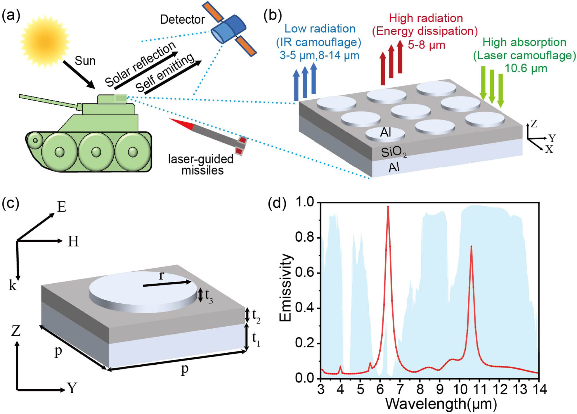
    Fig. 1. (a) Schematic of infrared detection process and laser guidance. (b), (c) Schematic of the designed infrared and laser compatible stealth nanostructure. (d) Simulated emissivity of designed nanostructures. The blue section is the transmittance spectrum of atmospheric windows in the mid-infrared band.
    Dependence of the simulated absorption spectra on different geometric structure with (a) the pitch length from 3 to 6 μm, (b) the radius of the top Al disk within the pitch from 1.0 to 2.0 μm, (c) the dielectric layer thickness from 0.10 to 0.30 μm, and (d) the height of the Al disk from 0.10 to 0.30 μm.
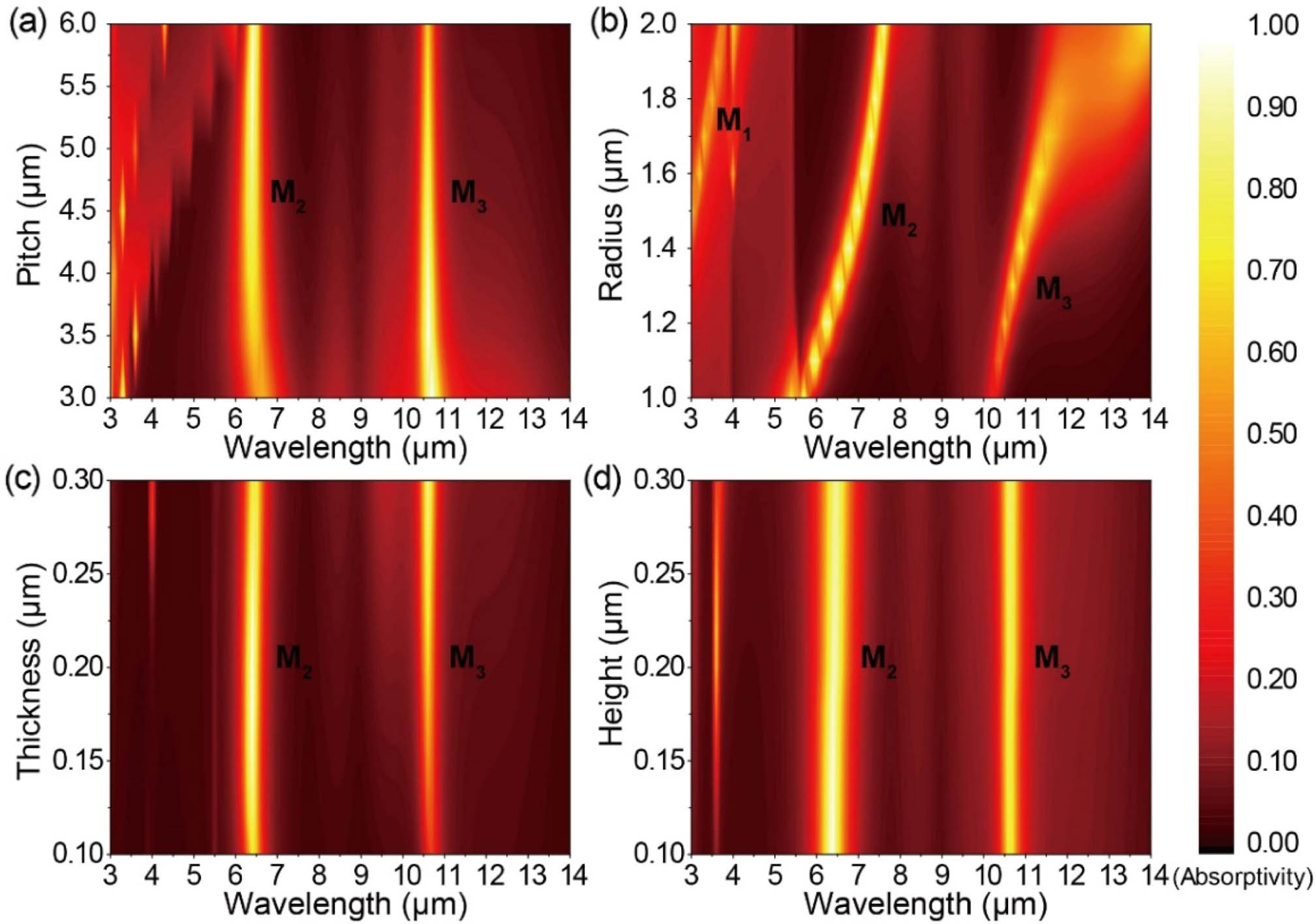
    Fig. 2. Dependence of the simulated absorption spectra on different geometric structure with (a) the pitch length from 3 to 6 μm, (b) the radius of the top Al disk within the pitch from 1.0 to 2.0 μm, (c) the dielectric layer thickness from 0.10 to 0.30 μm, and (d)  the height of the Al disk from 0.10 to 0.30 μm.
    (a)–(c) Simulated magnetic field intensity/electric field (the top row) and resistive loss/Poynting vector (the bottom row) at resonance wavelengths of 3.3 μm, 6.4 μm, and 10.6 μm, respectively. (d), (e) Simulated TE-mode (x-polarized) and TM-mode (y-polarized) absorption spectra for incident angles from 0° to 70°, respectively.
    Fig. 3. (a)–(c) Simulated magnetic field intensity/electric field (the top row) and resistive loss/Poynting vector (the bottom row) at resonance wavelengths of 3.3 μm, 6.4 μm, and 10.6 μm, respectively. (d), (e) Simulated TE-mode (x-polarized) and TM-mode (y-polarized) absorption spectra for incident angles from 0° to 70°, respectively.
    (a) Schematic of the fabrication process. (b) Photograph of prepared wafer-scale metasurface sample with diameter of 2.5 cm. (c) Top view and (d) cutaway SEM image of the fabricated sample (inset, magnified image of partial microdisk structure). (e) Spectral emissivity of the metasurface emitter measured by FTIR at different temperatures.
    Fig. 4. (a) Schematic of the fabrication process. (b) Photograph of prepared wafer-scale metasurface sample with diameter of 2.5 cm. (c) Top view and (d) cutaway SEM image of the fabricated sample (inset, magnified image of partial microdisk structure). (e) Spectral emissivity of the metasurface emitter measured by FTIR at different temperatures.
    (a) Schematic of the experimental setup for thermal infrared imaging and thermal management test; (b)–(g) infrared images and radiation temperatures of samples at different background (heating table) temperatures.
    Fig. 5. (a) Schematic of the experimental setup for thermal infrared imaging and thermal management test; (b)–(g) infrared images and radiation temperatures of samples at different background (heating table) temperatures.
    (a) Camouflage demonstration in infrared bands at room temperature; (b) spectral radiation of the sample, Al, and blackbody; (c) radiation temperatures of samples and high emissivity objects (silicon substrate) at different heating temperatures; (d) real temperature on the surface of the sample (red asterisks) and the Al film (black circles).
    Fig. 6. (a) Camouflage demonstration in infrared bands at room temperature; (b) spectral radiation of the sample, Al, and blackbody; (c) radiation temperatures of samples and high emissivity objects (silicon substrate) at different heating temperatures; (d) real temperature on the surface of the sample (red asterisks) and the Al film (black circles).
    Kun Yu, Wei Zhang, Mengdan Qian, Peng Shen, Yufang Liu. Multiband metamaterial emitters for infrared and laser compatible stealth with thermal management based on dissipative dielectrics[J]. Photonics Research, 2023, 11(2): 290
    Download Citation