Kun Yu, Wei Zhang, Mengdan Qian, Peng Shen, Yufang Liu, "Multiband metamaterial emitters for infrared and laser compatible stealth with thermal management based on dissipative dielectrics," Photonics Res. 11, 290 (2023)
Copy Citation Text
The modulation of thermal radiation in the infrared region is a highly anticipated method to achieve infrared sensing and camouflage. Here, a multiband metamaterial emitter based on the nanosandwich structure is proposed to provide new ideas for effective infrared and laser-compatible camouflage. By virtue of the intrinsic absorption and magnetic resonance property of lossy materials, the thermal radiation in the infrared region can be rationally modulated. The fabricated samples generally present low emissivity (μ, μ) in the atmospheric windows to evade infrared detection as well as high emissivity (μ) in the undetected band for energy dissipation. Additionally, the laser camouflage is also realized by introducing a strong absorption at 10.6 μm through the nonlocalized plasmon resonance of the layer. Moreover, the fabricated emitter shows promising prospects in thermal management due to the good radiative cooling property that is comparable to the metallic Al material. This work demonstrates a multiband emitter based on the metasurface structure with compatible infrared-laser camouflage as well as radiative cooling properties, which is expected to pave new routes for the design of thermal radiation devices.
1. INTRODUCTION
Thermal emitting devices in the infrared (IR) wavelength range have attracted increasing attention for their promising applications in atmospheric science [1–3], military [4–9], and energy engineering [10–12]. According to the Stefan–Boltzmann law, the thermal radiation signal intensity of target devices is determined by the temperature as well as emissivity. Compared to the precise control of temperature, changing surface emissivity is a more effective and convenient strategy to regulate the thermal radiation [13–15]. In consideration of the high transmittance at atmospheric windows [16], the emissivity of the target device at these two detection bands should be controlled as low as possible to make it invisible for active tracking systems, while the emissivity outside atmospheric windows remains high to ensure radiative heat dissipation. Modulation of thermal emission in the mid-IR (MIR) region plays an important role in IR camouflage technology, which aims to blend an object into the background environment by rationally modulating the radiative signals. Great efforts have been devoted to modulating the emissivity of objects to realize excellent IR camouflage performance [17–22]. Despite the enormous progress, the single-band IR camouflage still cannot cope with modern multispectral detecting technologies, and it is highly urgent to develop multiband compatible camouflage technologies for targets hiding under complex situations.
The difficulty with achieving multiband compatible camouflage is that the emissivity spectrum is quite different and even competing intrinsically in terms of different camouflage technologies. The advent of metamaterials provides new possibilities for the multiband emissivity modulation by adjusting electromagnetic behavior via microstructures [23–27]. Various types of camouflage strategies based on metamaterials have been proposed to enable the manipulation of electromagnetic energy and modulation of emissivity toward multiband compatible camouflage [28–32]. For instance, Zhong et al. demonstrated an artificial structure based on two metasurface layers for radar-IR compatible camouflage [33]. Though several metamaterials have been used for multiband compatible camouflage, the working wavelength mainly lies in the IR and microwave band [34–37], while the compatible laser and IR camouflage is rarely reported. As for the compatible camouflage, the IR camouflage requires low emissivity at atmospheric windows (3–5 μm and 8–14 μm), whereas high absorptivity is demanded at laser radar working wavelength (10.6 μm for laser radar). The conflicting emissivity requirements and overlapping wave bands make it challenging to achieve multiband laser and IR compatible camouflage.
Herein, a novel thermal emitter based on metal/insulator/metal (MIM) geometry with a combination of well-tailored metasurface structures is demonstrated to achieve multispectral camouflage and thermal management. The dissipative medium is introduced in the metamaterial structure to enhance the light absorption and consume the incident energy. The fabricated emitter has low emission at atmospheric windows (μ, μ), and good radar camouflage performance with high absorption at 10.6 μm due to the non-negligible inherent loss property in the MIR band of the silica dioxide dielectric layer. Besides, the prepared samples show low radiation temperature under the IR camera, lower than that of the conventional metal surface, indicating the excellent thermal cooling capability. Meanwhile, the metamaterial emitter has good thermal stability with little variations in the emissivity spectrum when the measurement temperature ranges from 150°C to 350°C. The work provides new ideas for the future design of a simple metamaterial emitter toward multiband compatible camouflage and thermal management.
Sign up for Photonics Research TOC. Get the latest issue of Photonics Research delivered right to you!Sign up now
2. RESULTS AND DISCUSSION
A. Structure Design and Simulation for a Selective Thermal Emitter
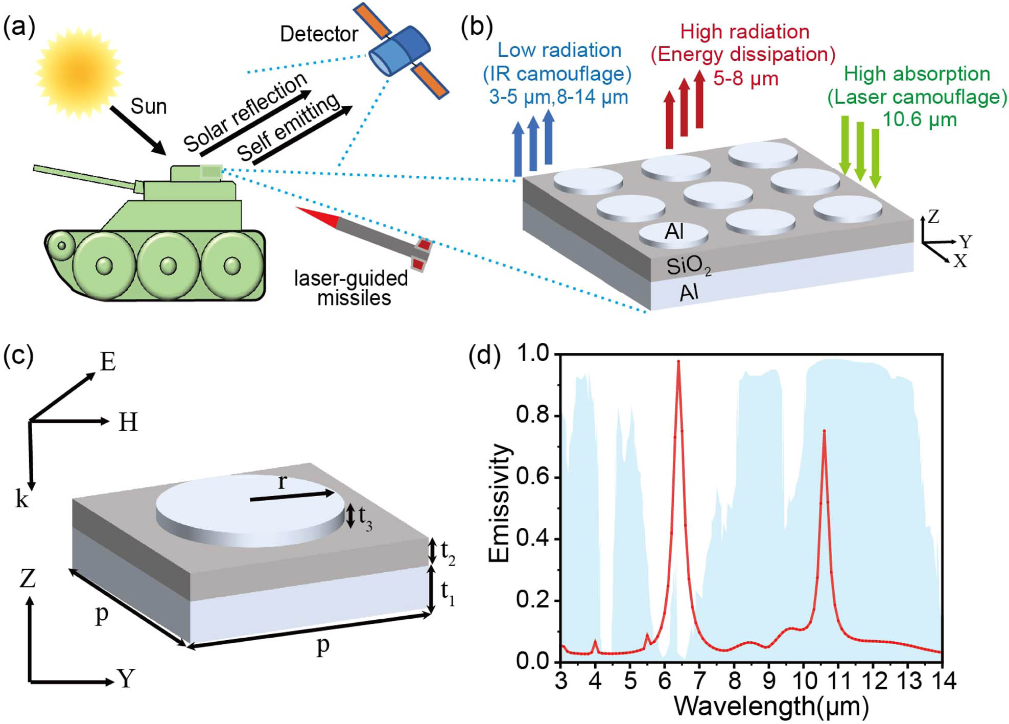
The emitted energy can be maximized by virtue of lossy materials with strong dispersion property in a certain wave band [38]. Different from previously reported emitter structures that usually use lossless materials (such as [26], ZnS [4,5,34]) in IR regions, silica dioxide is mainly chosen as the dielectric spacer in radiation cooling due to its inherent lossy properties in the MIR band [39–42]. Among various types of selective emitters, the three-layer MIM configuration shows enormous potential for IR camouflage because of the simple structure and selective emission capacity [43,44]. Figure 1(a) shows the conceptual scheme of the designed selective emitter that is expected to have compatible functionality in IR-laser stealth as well as thermal management. Specifically, Al is used as the metal layers for the high reflectance and the low emittance trait in the MIR region, and the top Al layer is designed to be periodic resonator arrays to allow tunability of the surface emissivity spectrum. For the dielectric layer, the lossy material silicon dioxide () with specific refractive index imaginary part value is chosen to absorb the partial incident light at targeted wave band. The local magnetic resonance generated in MIM structure maximizes the emission energy at the lossless region of 3–8 μm, which corresponds to the atmospheric absorption window. The loss region gives excitation of intrinsic absorption of 8–14 μm, which can be coupled with plasmonic resonance of the metasurface structure to enhance absorption at a certain band. Prior to the structural fabrication and measurement of the selective thermal emitter, numerical simulation on the absorption performance and electromagnetic distribution of the metamaterial emitter is performed by COMSOL Multiphysics software. In each period cell of metasurface structure, the thickness () and radius () of the top Al disks are set as 100 nm and 1.25 μm, respectively, and the period of the emitter is 5.5 μm in Fig. 1(c). The bottom reflective mirror is the Al layer () with a deposition of 220 nm thick as the dielectric layer. The simulated spectral absorption of thermal emitter based on the above parameters is depicted as Fig. 1(d) (red line). It is clear that the emitter generally maintains low emissivity at 3–5 μm and 8–14 μm atmospheric windows, which is favorable to IR camouflage due to the similar low absorption of atmospheric background in this IR band. Notably, a narrow absorption peak appears at 10.6 μm, a typical band for laser detection, which can be attributed to the coupling plasmonic resonance of metallic microstructures. Meanwhile, the spectral emissivity is high in the undetected band (5–8 μm) where the radiation energy accumulated in the non-atmospheric window can be effectively dissipated to maintain the thermal stability of the emitter system. Overall, the designed metasurface emitter generally has a low IR emissivity in the atmospheric window to satisfy the emissivity demand of IR camouflage, while it presents relatively high emission intensities at the undetected IR wavelength (5–8 μm) for efficient thermal dissipation as well as high absorption intensities at the radar operating wavelength (μ) for laser camouflage.
Figure 1.(a) Schematic of infrared detection process and laser guidance. (b), (c) Schematic of the designed infrared and laser compatible stealth nanostructure. (d) Simulated emissivity of designed nanostructures. The blue section is the transmittance spectrum of atmospheric windows in the mid-infrared band.
The absorption behavior of designed metasurface emitters is susceptible to the geometric configuration. In order to further understand the electromagnetic behavior, numerical analysis of spectral information and electromagnetic distribution on the dependence of geometrical factors is subsequently performed. Figures 2(a)–2(d) show the simulated absorption spectra of emitters under different geometric parameters. According to the results, the resonance wavelength is closely related to the geometric size. It is noted that the variation of pitch and radius of the metallic disk array can affect the position as well as the intensity of absorption peaks. As the pitch size increases from 3 to 6 μm, the resonant wavelength at 5–8 μm ( band) shows a slight blueshift along with the enhanced absorbance intensity in Fig. 2(a). Remarkably, a continuous redshift of the resonant wavelength from 5 to 8 μm ( band), a virtually undetected zone for IR devices, is observed with the increasing radius of the Al disk at 1–1.4 μm. Meanwhile, the absorbance intensity becomes stronger, and the wavelength moves from 10 toward 11 μm ( band). When the disk radius exceeds 1.4 μm, the resonant wavelength of 3–5 μm ( band) begins to appear, and the band becomes broader and weaker in Fig. 2(b). Variation of dielectric layer thickness can change the absorption intensity at band, while the height of the metallic disk has little impact on the absorption spectra in Figs. 2(c) and 2(d).
Figure 2.Dependence of the simulated absorption spectra on different geometric structure with (a) the pitch length from 3 to 6 μm, (b) the radius of the top Al disk within the pitch from 1.0 to 2.0 μm, (c) the dielectric layer thickness from 0.10 to 0.30 μm, and (d) the height of the Al disk from 0.10 to 0.30 μm.
Subsequently, the electromagnetic behaviors at the three resonant wavelengths of 3.3, 6.4, and 10.6 μm are simulated, respectively, to investigate the coupling resonance modes of the emitter in Figs. 3(a)–3(c). At the resonant wavelength, the incident electric field induces contrary charge distribution between the top and bottom Al dipoles, and the antiparallel induced current generates the magnetic field concentrated in the dielectric region between the bottom Al metallic reflector layer and the top Al disk. It is obvious that both the heat loss and electromagnetic field are mainly distributed in the medium layer sandwiched by the upper and lower metal layers. In Fig. 3(a), the magnetic field of resonance wavelength at 3.3 μm () is confined within the intermediate dielectric layer between the bottom Al layer and top Al microdisk, indicating the generation of typical third-order magnetic resonance in the submicron MIM structure. In consideration of the camouflage requirements, this high-order magnetic resonance should be minimized to reduce the thermal radiation signal at the atmospheric window. Besides, a localized low order of magnetic resonance is observed at the resonant wavelength of 6.4 μm (), and the high absorption at this band is desirable for the essential energy dissipation in IR camouflage.
Figure 3.(a)–(c) Simulated magnetic field intensity/electric field (the top row) and resistive loss/Poynting vector (the bottom row) at resonance wavelengths of 3.3 μm, 6.4 μm, and 10.6 μm, respectively. (d), (e) Simulated TE-mode (-polarized) and TM-mode (-polarized) absorption spectra for incident angles from 0° to 70°, respectively.
Except for the magnetic resonance at and , a strong absorption peak is also observed at band of 10.6 μm. As the simulation results show in Fig. 3(c), it has weaker magnetic field intensity but basically identical electric field distribution to resonance. The resonant absorption at comes from nonlocalized magnetic resonance. The nonlocalized plasmon behavior can be further validated by the absorption spectrum in Fig. 2(b), where the absorption peak at gradually becomes divergent as the radius of the metallic microdisk has large variation beyond 1.5 μm. Furthermore, the nonlocalized plasmon resonance at is attributed to the anomalous dispersion by the lattice vibration of dielectric layer (), which is related to the complex refractive index. In terms of the lossy material , the real part () of the refractive index dominates the impedance matching while the imaginary part () is related to the excitation of intrinsic absorption at band. The anomalous dispersion of dielectric layer can induce the additional impedance matching at band and further affects the spectral emissivity of the MIM emitter in IR spectrum. Notably, the imaginary part of the refractive index () is supposed to be associated with the dielectric thickness for the reason that the resonant absorption intensity in becomes intense as the thickness of the dielectric layer gradually increases in Fig. 2(c). Additionally, rational modulation of metallic unit structures also contributes to the coupling of nonlocalized magnetic resonance peak at 10.6 μm to match the laser detection. The selective emission in the IR band and the strong absorption in the laser band can be, respectively, attributed to the magnetic resonance between the metal and dielectric layer as well as the inherent loss property of the anomalous dispersion medium (). Taking all factors into consideration, the pitch length, radius, and dielectric thickness are set as 5.5, 1.25, and 0.22 μm to ensure the high emissivity at 6.4 μm as well as desirable absorption at 10.6 μm for compatible IR and laser stealth.
The absorption spectra of the designed MIM emitter at different incident angles are calculated to validate the feasible camouflage performance over different observation angles. The dependence of absorptivity for both transverse electric (TE) polarization and transverse magnetic (TM) polarization at oblique incidence is shown in Figs. 3(d) and 3(e), respectively. When the incidence angle is less than 40°, the absorption spectrum remains almost unchanged in terms of both polarizations, presenting almost angle-independent absorption for both TE and TM modes, whereas continuous increase of the incident angle results in distinctly different spectral behavior of TE-polarized and TM-polarized absorptivity. As the incidence angle increases beyond 40°, the resonant absorption in TM polarization is excited at the wavelength of about 8 μm, while this phenomenon is not observed in the TE case. The angle-dependent absorption in TM polarization near 8 μm is associated to the Berreman wavelength of , which has been validated in the previously reported experiment [45,46]. Therefore, the emitter spectral absorbance remains insensitive to the polarization of the incident light over a wide angular range. The detector can detect the target by changing the incident angle and polarization state, while the emitter maintains low spectral emissivity in the detection band and high absorption in the laser operating band over a wide range of 40°, which means that the susceptibility of the target is reduced and contributes to the improved target survivability of designed emitter.
B. Fabrication and Infrared Camouflage Demonstration
In order to validate the simulated results, the designed MIM emitter is then fabricated, and its compatible camouflage performance is also discussed in this section. The fabrication process of the emitter is shown in Fig. 4(a). The bottom Al layer and layer are deposited on the glass substrate by electron beam evaporation, and the top metal pattern is prepared by a lift-off lithography process. Figure 4(b) shows the photograph of wafer-scale sample with microdisk arrays, in which the colored part of the sample is the structural region. The morphology of metasurface geometry is characterized by a scanning electron microscope (SEM). As shown in Fig. 4(c), the metallic microstructures are uniformly distributed with a smooth surface and the same periodic length. Besides, the thickness of the Al disk, , and Al layer and the diameter of the Al disk are approximately 100, 220, 300, and 2.5 μm, respectively, as observed from the cross section of an individual unit cell from top to bottom in Fig. 4(d). All these structural data indicate that the metasurface emitter is successfully constructed with corresponding parameters as the theoretically designed one.
Figure 4.(a) Schematic of the fabrication process. (b) Photograph of prepared wafer-scale metasurface sample with diameter of 2.5 cm. (c) Top view and (d) cutaway SEM image of the fabricated sample (inset, magnified image of partial microdisk structure). (e) Spectral emissivity of the metasurface emitter measured by FTIR at different temperatures.
The thermal stability of the prepared metasurface sample is also investigated by measuring the spectral emissivity under different temperatures. Figure 4(e) gives the emissivity curves of the emitter with sample temperatures ranging from 150°C to 400°C. It is clear that the emissivity spectra have little variation as the temperature increases to 350°C, while enhanced emissivity is observed on the emitter sample when the temperature reaches 400°C. The little difference of the measured sample in emission spectra between 150°C and 350°C indicates its highly stable radiative property under temperature variation. For a certain temperature , the average emissivity of the sample in the specific wavelength band can be expressed by the spectral emissivity and blackbody irradiation as follows: in which is the spectral irradiance of the blackbody, and represent the band range, is the emitter emissivity, and , , , and are the Planck’s constant, the speed of light in vacuum, the Boltzmann’s constant, and temperature, respectively. According to the above equations, the average emissivities below 150°C in the 3–5 μm, 5–8 μm, and 8–14 μm bands are calculated to be 0.21, 0.43, and 0.19, respectively. Generally, the measured emissivity curves in experiment are in good consistence with the simulated result in terms of characteristic resonant peak position. Nevertheless, the emissivity intensity at a typical resonant wavelength of 10.6 μm is slightly lower than the simulated value, which might result from the geometric deviation during the fabrication process of metasurface devices. Furthermore, according to the analysis of the absorption mechanism of the emitter in the previous section, the actual refractive index of the prepared might be different from the data employed in the simulation, which is responsible for the partial intensity deviation at the resonance wavelength. Taking all these factors into consideration, the fabricated devices have similar working performance with designed emitters and basically meet the demand of IR-laser compatible camouflage.
The IR camouflage performance of the emitter is demonstrated through IR images recorded by the self-built test system as shown in Fig. 5(a). The thermographic images of the fabricated sample, together with silicon substrate (high emissivity objects: ) as a comparison reference, are captured by the IR camera, from which we can intuitively observe the camouflage effectiveness. The IR images of the prepared sample on the heating table with the temperature ranging from 102°C to 280°C are shown in Figs. 5(b)–5(g). As shown in Fig. 6(a), the radiative temperature of the sample () under the IR camera is lower than that of the human body (), while it has a similar radiation signal with the surrounding environment, indicating that the sample is almost invisible under the MIR camera at room temperature conditions. As shown in Fig. 6(c), as the heating temperature gradually increases from 50°C to 240°C, the radiative temperatures of both the sample and reference rise accordingly. The radiation temperature of the sample exhibits a small variation from 30°C to 60°C, much lower than that of the silicon substrate, which increases by about 160°C (40°C–200°C) under the heating process. When the heating temperature increases to 240°C, the radiative temperature of the silicon substrates reaches 202.6°C while the sample only has a low temperature value of 67.5°C. As the heating temperature increases, the radiation temperature of the sample gradually grows up with a much lower growth speed than that of the background heating table, which is attributed to the low emissivity property of the designed emitter in the IR camera’s operating band (7.5–14 μm). The recorded IR images reveal that the sample shows low visibility in the IR camera despite a higher surface temperature, reducing the possibility of being detected in IR camouflage.
Figure 5.(a) Schematic of the experimental setup for thermal infrared imaging and thermal management test; (b)–(g) infrared images and radiation temperatures of samples at different background (heating table) temperatures.
Figure 6.(a) Camouflage demonstration in infrared bands at room temperature; (b) spectral radiation of the sample, Al, and blackbody; (c) radiation temperatures of samples and high emissivity objects (silicon substrate) at different heating temperatures; (d) real temperature on the surface of the sample (red asterisks) and the Al film (black circles).
In consideration of the low emissivity of the fabricated thermal emitter, it is also expected to have promising applications in thermal management. The excellent radiative cooling property of the prepared sample makes it useful not only for IR camouflage but also for thermal management owing to its strong radiative ability at undetected wavelengths. The thermal management performance is demonstrated by comparing the spectral radiation of the sample with an equal-sized Al film as the reference. Figure 6(b) shows the spectral radiation of the blackbody, emitter sample, and Al film at 150°C, from which the radiated power of the sample can be obtained. The radiated power of the sample is estimated to be at 3–5 μm and at 8–14 μm, which is much lower than that of the blackbody with the value of and , respectively. In contrast, the Al film exhibits the smallest radiated power because of the ultra-low spectral emissivity () during the IR band, which can be attributed to the intrinsic dissipated property of Al. The emitter sample has a dissipated power of through the undetected IR band (5–8 μm), which is 328.68% higher than that of the Al surface. It is the high dissipated power of the designed emitter that is responsible for the promising application in thermal management.
The thermal management performance by radiative cooling is further demonstrated by comparing the real temperature of the sample and Al film under different ambient temperatures. The samples are heated by the heating table, and the surface temperature can be precisely measured by the thermometer connected with a thermocouple [Fig. 5(a)]. Figure 6(d) shows the surface temperature of both the fabricated samples and Al film increased with the increasing in heating temperature. When taking Al film as the reference, the real temperature of the sample generally shows similar variation trends but always a little smaller value because the radiated power from the sample is greater than that from Al film at the non-atmospheric window. Specifically, with the heating temperature of 250°C, the real temperature of the sample (206.1°C) is 4.7°C lower than that of the Al film (210.8°C), indicating the comparable good thermal management performance of the sample. The thermal management performance of the metasurface sample can be ascribed to its good capacity to dissipate the accumulated energy from atmospheric window regions to the undetected band, which contributes to the excellent thermal management performance with radiative cooling at high temperatures.
3. SIMULATION AND EXPERIMENTAL SECTION
The numerical simulations were performed in the commercial solver, COMSOL Multiphysics v.5.5. The refractive index-related information of Al [47] and [48] was obtained from previously reported literature. In each simulation calculation cell, the absorptivity of the emitter is calculated by collecting the scattering parameters , [49], and the band range studied is 3–14 μm. From Kirchhoff’s law, , where , , , and are the emissivity, the absorptivity, reflectivity, and transmissivity, respectively. The skin depth of electromagnetic waves in the metal is much smaller than the thickness of the continuous metal film at the bottom of the structure in the studied IR band, so can be approximately regarded as zero, and then the calculation of the emissivity simplifies to .
Regarding multiband metamaterial emitter fabrication, first, a 1 mm thick glass wafer was cleaned with acetone, sonicated for 3 min, and sequentially rinsed with ethanol and deionized water to remove organic matter from the glass wafer. The 150 nm Al layer and 220 nm layer were successively deposited by an electron beam evaporator. The fabrication of top patterned Al array disks can be fabricated by the lift-off technique. Then, through a spin-coating photoresist process [(i) 500 r/min for 5 s; (ii) 3000 r/min for 20 s; (iii) 5000 r/min for 10 s], photoresist (AZ5214E) was coated to the prepared sample’s surface and baked at a constant temperature of 100°C for 60 s. The sample coated with photoresist was covered by a lithography mask and then exposed under straight halogen lamp light for 25 s to etch patterning photoresist by the URE-2000/35 lithography machine (Institute of Photoelectric Technology, Chengdu, China). Subsequently, the sample with photoresist was immersed in the NMD-3 developer for 60 s to remove the exposed region. A 100 nm thick Al film was deposited onto the prepared sample using an electron beam evaporator, and then the sample was immersed in NMP stripping solution for removing the redundant Al layer and photoresist. Finally, the multiband metamaterial emitter was fabricated.
For IR emissivity and thermographic measurement, the emittance spectra of the sample were obtained by a Fourier transform infrared (FTIR) spectrometer (Bruker 70 V) with a liquid-nitrogen-cooled mercury cadmium telluride (MCT) detector and a KBr beam splitter. The blackbody (IR-563) was used as a standard radiation source. The normal spectral emissivity of the sample is calculated by the following formula: where , , and are the radiation intensities of the sample, blackbody, and background at the same temperature , respectively. The temperature of the sample was directly controlled by the heating table and monitored with thermocouples, and the thermographic images were measured by an IR camera (TiX640, μ, to 1200°C, FLUKE) for observing the radiation temperature of the sample at different heating temperatures. The SEM image of the samples was obtained with the field emitted scanning electron microscopy (FESEM) (SUPRA40, Zeiss, Germany).
4. CONCLUSION
In summary, we demonstrate a novel metamaterial emitter that is compatible with both IR and laser camouflage as well as thermal management. The composite emitter structure is composed of a metal Al film at the bottom, as the dielectric layer in the middle, and the Al disk array on the top. The low-order magnetic resonance wavelength excited by the specific MIM structure is used for the selective thermal emission in the IR band, while the inherent loss of dielectric medium is excited to cause high absorption in the laser operating band for laser camouflage. The combination of inherent material properties and special structure cleverly solves the compatibility problem of multiband stealth at IR and laser regions. Furthermore, the fabricated emitter is expected to have good thermal management performance because of the radiative cooling caused by energy dissipation at the undetected band. Above all, the designed metasurface emitter based on lossy media possesses substantial viability in selective spectrum modulation, stimulating new possibilities for energy conversion, thermal management, and stealth applications.