Waveguide superlattices, a special type of waveguide arrays, can be designed to achieve very low cross talk at submicrometer/subwavelength pitches. The theoretical framework and design rationales for such waveguide superlattices will be presented in depth. Waveguide sidewall roughness can help to deter the coherent coupling between identical waveguides in nearby supercells, but it also induces random fluctuation of transmission. Statistical behavior of the transmission due to roughness in a waveguide superlattice is systematically treated. Complex transmission characteristics due to spectral oscillation and random roughness will be presented, and their evolution with the superlattice length will be analyzed.Institutions.
Waveguides are ubiquitous in integrated optics. The density of waveguides is a fundamental issue in many integrated optical devices and systems. High-density waveguides with small pitch are often preferred in many applications. For example, in a wavelength demultiplexer or spectrometer based on echelle gratings [1], the wavelength resolution can be directly enhanced by increasing the density of the output waveguides. For an optical phased array, high-density output waveguides with half-wavelength pitches would be ideal [2,3] for wide beam steering range and high energy efficiency. Furthermore, with the recent rise of silicon photonics [4–10], chip-scale optical interconnection is envisioned. Future computer chips with more than 100 cores may require tens of thousands of waveguide channels for interconnection [11]. The density of waveguides will be crucial to reducing the on-chip estate occupied by the waveguides and to reducing the associated cost. Previously, dielectric waveguide density is fairly low, with pitches a few micrometers or more [12–14]. Recently, high-density waveguide superlattices with half-wavelength pitches have been proposed and demonstrated [15,16]. This work will present detailed theoretical analysis and design rationales that enabled the development of such waveguide superlattices. Note that coupling in densely packed waveguides has also been analyzed with insight from atomic physics analogy [17]. Artful designs of thermo-optic switches have been proposed and demonstrated using densely packed waveguides to greatly reduce the switching power [18]. Ingenious schemes of simultaneous mode and polarization-division multiplexing have been proposed and demonstrated in densely packed waveguides [19].
2. SUPERLATTICE CONCEPT AND DESIGN CONSIDERATIONS
A. Prior Approaches
If we are interested in reducing the cross talk between two waveguides only, there is a simple approach based on directional couplers. In an asymmetric directional coupler, the intercoupling between two waveguides can be very low if the propagation constant difference of the two waveguides is sufficiently large. According to the well-known theory for directional couplers [20], the coupling ratio is given by , where is the coupling length and κ the coupling strength. If , the coupling ratio (i.e., cross talk) can be less than . However, just as the technique of forming a molecule cannot be applied to form a hydrogen crystal, the above method for two waveguides cannot be applied to a large array of waveguides. Fundamentally, this is because in a large array, substantial intercoupling of waveguides exists between the second-nearest and third-nearest neighbors and beyond. At large waveguide pitches, such couplings between nonnearest-neighbors is negligible, but they can exhibit themselves prominently as the waveguide pitch reaches the subwavelength (sub-) scale. Furthermore, direct couplings can cascade to form a sequence of indirect coupling paths. The superposition of these direct and indirect paths can result in very complex cross-talk behavior with respect to the neighboring waveguide index. Cross talk may not decrease monotonically with waveguide-index difference. For example, sometimes the cross talk to a second-nearest neighbor can be higher than that to the nearest neighbor. An example can be found in the Supplementary Information of [16]. To block all these direct and indirect coupling paths, new approaches need to be explored.
Some other approaches were also considered to reduce the cross talk in waveguide arrays. For example, decoupling of densely packed photonic crystal waveguides has been observed in simulation, which can be explained by the self-imaging principle [21]. Photonic crystals inserted between waveguides were found to help reduce the cross talk experimentally [22]. However, the insertion of the photonic crystal structures requires additional space between waveguides and limits the smallest achievable pitch. It is also possible to modify the propagation constants along the waveguide axis. But this generally causes additional insertion loss and sometimes causes backscattering of light. A preferred approach is to maintain a uniform cross section along the axis of each waveguide while varying the widths among different waveguides. It is also possible to vary the waveguide height. However, from the fabrication point of view, varying the waveguide height will require additional fabrication steps and incur higher cost.
Sign up for Photonics Research TOC. Get the latest issue of Photonics Research delivered right to you!Sign up now
B. Design Constraints
Once the avenue of varying waveguide width is chosen, there remain a number of constraints that fundamentally limit the design of a waveguide array with low cross talk. First, most applications require each waveguide to operate in the single-mode regime, which poses an upper bound for the waveguide width. Second, as the waveguide narrows below a certain critical width (e.g., 300 nm), the mode width expands significantly, which causes increased mode overlap and enhanced inter coupling/cross talk with other waveguides in an array. This results in a lower bound for the waveguide width. Third, between the upper and lower bounds of widths, a number of widths can be chosen to design the waveguides. However, generally it is preferred that the waveguide widths are sufficiently different; otherwise there may be difficulties in fabricating the structures with sufficient tolerance.
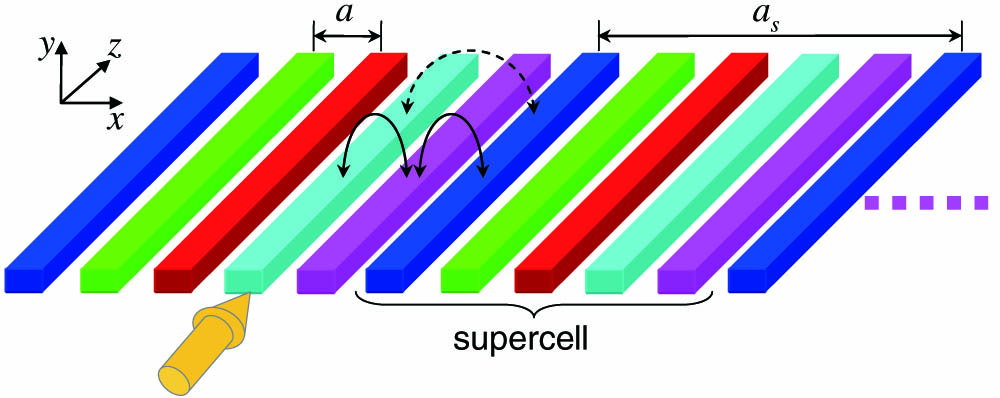
Under these constraints, there are two possible categories of structures: (1) a waveguide superlattice where the waveguide widths repeat periodically every waveguides as illustrated in Fig. 1; (2) a random waveguide lattice where the waveguide widths have no clear order.
Figure 1.Schematic drawing of waveguide superlattice structure. Direct coupling path and indirect coupling paths are illustrated by dashed and solid lines.
Figure 2.Dielectric constant profile for (a) the superlattice, (b) an isolated waveguide #4, and (c) the dielectric perturbation corresponding to the perturbation potential .
Light localization in random (or disordered) photonic structures has been studied for decades [23–25]. In principle, when a one-dimensional photonic lattice is random, light will be localized. For an array of waveguides whose propagation constants are all random, it is anticipated that all waveguides will be localized around certain waveguides. This suggests the decoupling of waveguide modes, which has potential to be applied to reduce the cross talk.
However, a number of issues in waveguide applications limit the viability of such a randomization approach. First, localization theory generally cannot guarantee that each waveguide mode has a localization length less than one lattice constant (in terminology of localization) or that each mode is localized around just one waveguide (in terminology of waveguides). Indeed, sometimes, a localized mode can spread over two or more lattice sites [26]. Second, even for a mode that has a localization length less than one lattice constant, such a mode usually has some overlap with adjacent lattice point (or waveguides). It is difficult to guarantee, for each mode, such overlap is weak enough to produce cross talk, which is often required for photonic applications. In addition to randomization, other light localization approaches, such as curved waveguide arrays [27], may also be useful to reducing cross talk. More studies are needed to explore these scientific approaches to assess whether they meet the cross-talk requirements (usually in dB scale) for practical applications at subwavelength pitches.
3. THEORY OF WAVEGUIDE SUPERLATTICES
This section presents the theoretical framework used in waveguide superlattice design.
A. Theory of a Waveguide Superlattice
Here we present a waveguide coupling theory for high-index-contrast waveguides (such as waveguides), built upon a prior cross-sectional mode theory in a photonic crystal waveguide. A general full-vectorial form of the cross-sectional mode theory is given as follows [28]: where is the dielectric function, the permeability, and the angular frequency of light. The axes of waveguides are along the axis. For an array of waveguides, the tensorial potential is given by , where is the tensorial potential for a homogeneous system with the index of the cladding material (e.g., the entire space is filled with ). The tensorial potential for an isolated waveguide is given by , whose corresponding index profile is plotted in Fig. 2(b).
For an isolated structure that has the th waveguide only, the mode solution is given by where satisfies . Note that the th waveguide’s cross section is centered at with a width . The mode orthogonality is given by , where is the optical power of the mode. This is based on For a guided mode, . A mode of a waveguide array can be expressed in the form of This form of mode can be substituted into Eq. (1) to find a set of equations for the coefficients as follows: From Eq. (5) onward, we will neglect the backward guided modes, whose propagation constants are negative and differ greatly from the propagation constants of the forward guided modes (). Because of the large difference in between forward and backward modes, the cross talk between them is usually orders of magnitude smaller than the leading cross-talk terms between forward modes. One can readily see this through the asymmetric directional coupler formula above. The matrix can be considered as a perturbation. Therefore we can define a perturbation matrix whose elements are For the fourth column of , the corresponding dielectric constant perturbation for is shown in Fig. 2(c). Note that the corresponding dielectric constant “perturbation” is not small in space. This is the nature of silicon photonic structures due to their high index contrast. Therefore, we cannot make simple approximations based on small index perturbation. It should also be noted that the spatial profile of the perturbation varies with the column index . For example, for the fifth column of , the “missing waveguide core” would be at the fifth waveguide location, corresponding to .
The coefficients can be solved from the following equation: The final field amplitude (envelope function) in the th waveguide is given by The corresponding optical power in each waveguide can be calculated accordingly, and Eqs. (7) and (8) can be used to assist in designing waveguides with high density.
Sometimes, it is more convenient to introduce a phased mode coefficient, where represents a reduced phase variation (removing a fast varying term). The coefficient satisfies a simpler equation, where . The [] matrix will provide more convenience in subsequent discussions.
Generally, the coupling generally will cause the propagation constants of the supermodes to deviate from the propagation constants of the isolated waveguides. It would be interesting to know how much deviation it can cause and whether this can lead to two supermodes having very close propagation constants, which often leads to high cross talk. Based on the Gershgorin circle theorem [29], the eigenvalues of [] should satisfy Thus, the sum of all off-diagonal elements on each row, , is sufficiently small, and should be very close to . Note that is essentially the propagation constant of the th supermode, and is roughly the propagation constant of the waveguide . When the sum of the coupling terms on the right-hand side of Eq. (11) is small, this equation indicates that the propagation constant of a supermode will not deviate far from that of an isolated waveguide. Generally, the off-diagonal matrix element behaves as for sufficiently large values of , where is roughly a constant. The exponential decrease with ensures that the sum converges.
In addition, one readily sees that By virtue of Eq. (11), one can readily show that Therefore, if the following condition is satisfied, Eq. (13) shows that the propagation constants of the supermodes are sufficiently different.
However, in a superlattice where some waveguides inevitably have the same propagation constant and hence the same , Eq. (14) can no longer be satisfied for some and in an ideal structure. To suppress the cross talk due to such degenerate modes, nonideal effects in a real waveguide superlattice must be considered, as discussed next.
B. Roughness-Induced Effect in a Waveguide Superlattice
In real waveguides, roughness generally adds a random perturbation to the mode equation, Eq. (7): where [] represents the roughness-induced perturbation potential. Each element of [] is a function of ; usually only its correlation function is known. The perturbation potential [] is dominated by the diagonal term, which gives a random correction of propagation constant, , for the th waveguide. The off-diagonal element of is a factor smaller ( for , even smaller for larger pitches), where is the off-diagonal term of normalized [] (i.e., diagonal elements are all unity). The random roughness has two effects. First, the diagonal elements, , lift the degeneracy between superlattice modes that would otherwise have identical propagation constants in an ideal roughness-free structure. Physically, it produces a phase dither as the wave propagates in each waveguide. This prevents coherent cross talk between waveguides with identical widths. Second, the off-diagonal elements produce random scattering, which creates additional incoherent cross talk.
For the coefficient , the following equation applies: where . Note that because the off-diagonal elements [] are much smaller than the diagonal ones, is nearly diagonal as well.
If [] and commuted with each other, one can obtain which would greatly facilitate the statistics calculation of the output intensity and cross talk for small roughness. Unfortunately, because elements of [] depend on , even if we assume that is diagonal, [] and do not commute with each other. Hence, there is no simple way to integrate Eq. (16) analytically, and the statistics must be numerically calculated with a large number of random configurations. This requires extensive numerical simulations using the theoretical formulation in this work. Note that the above theory only needs discretization along whereas the commonly used method such as the finite-difference time-domain (FDTD) technique needs discretization in , , and . The above theory is much more efficient. If the FDTD technique is used, the simulation time could be prohibitive considering the waveguide length and simulation grid needed for simulating small roughness. Note that the effect of stochastic variation of the widths of a two-waveguide coupler have been studied by other methods recently [30]. Note that radiation modes are neglected here, considering prohibitive computational resources needed for calculations involving a huge number of radiation modes [28]. Generally, only the cross talk between guided modes is of interest; therefore radiation modes are not essentially needed in cross-talk calculation. The role of radiation modes is primarily to produce optical loss through roughness-induced scattering. The effect of such loss can be evaluated separately [16].
4. NUMERICAL RESULTS AND DISCUSSION
Based on the design constraints in Section 2.B, we have set the waveguide widths between a lower bound of 330 nm and an upper bound of 450 nm. The minimum width difference is set to 30 nm. Under these constraints, we consider a SC5 superlattice, whose supercell consists of waveguides with widths 450, 390, 330, 420, and 360 nm at a pitch of 800 nm.
Such a so-called interlacing-recombination configuration [16] can separate two waveguides with the smallest width difference by rather than , which effectively reduces the cross talk between them. The statistical transmission characteristics for such an SC5 superlattice are shown in Figs. 3–5 for superlattice lengths μ, 1 mm, and 3 mm, respectively. RMS roughness and correlation length are taken from [16].
Figure 3.Statistics of transmission fluctuation (indicated by error bars) for an SC5 superlattice, , , , μ.
For each cross-talk channel , the peaks of the averaged transmission spectrum change insignificantly with the superlattice length after a short stabilization length (typically μ). For example, the peaks of the averaged transmission spectra for μ, 1 mm, and 3 mm are , , and . Here indicates an average over all random configurations. The error bars in Figs. 3–5 indicate one standard deviation.
The random distributions of transmission for a typical cross-talk channel at given wavelengths and lengths are shown in Fig. 6. The distributions vary with wavelengths and lengths. Spectra of several random configurations are shown in Appendix A.
Figure 6.Distribution of at given wavelength (nm) and (μm). Plots in each row have the same ; plots in each column have the same .
Furthermore, the magnitude of the random fluctuation of changes significantly with . For a given , the standard deviation over all random configurations of roughness is not necessarily a monotonically increasing function of , as shown in Fig. 7(a)—using as an example. In the absence of roughness, the deterministic transmission spectra of an ideal waveguide array comprise nearly periodic undulations. These deterministic spectra agree very well the averaged spectra of waveguides with roughness, as expected. As increases, the periodicity of the spectral undulation changes, and the spectral peaks and valleys of shift. Depending on whether a given is close to a peak or valley, the sensitivity of to small roughness varies substantially. The overall trend of in Fig. 7(a) is that it increases with , albeit there are significant fluctuations. Note that such fluctuations are for the standard deviation of , not itself. The magnitude of such fluctuations increases monotonically for μ, but it does not show a clear trend of increase/decrease for large in Fig. 7(a). In addition, the increase of slows down for .
Figure 7.Statistical characteristics of the transmission as a function of . (a) Standard deviation of over all random configurations at three individual wavelengths. (b) Statistical characteristics of calculated over all random configurations of roughness and over all wavelengths.
Interestingly, if the statistical transmission characteristics are calculated over all random configurations of roughness and over all wavelengths (indicated by ), the results show a more consistent trend of slow increase without much fluctuation (after the initial stabilization length), as shown in Fig. 7(b). Clearly, the error bar length does not fluctuate significantly with . This seems to indicate that when all fluctuations due to random roughness and due to wavelengths variation are considered, a statistically stable ensemble is obtained. Furthermore, our calculations indicate that for large , the average transmission saturates toward a final value.
The theory in this work is applicable to waveguide arrays with pitches of half-wavelength or larger, which were experimentally studied in [16]. It would be interesting to further investigate waveguide arrays with even smaller pitches (e.g., corresponding to interwaveguide gaps of 100 nm or below). For such small gaps, some adaptation of part of the current theory may be beneficial [for example, one might directly solve the original mode equation, Eqs. (1) and (2), to find the supermodes]. Detailed analysis is beyond the scope of this work.
5. CONCLUSION
In summary, we have presented the design rationales and detailed theory of waveguide superlattices with subwavelength/submicrometer pitches. Prior approaches to cross-talk reduction have been briefly discussed. The concept and theoretical formulation of low-cross-talk waveguide superlattices are then developed. The spectral dependence of cross talk at various superlattice lengths has been presented. The complex behavior of such dependence with random transmission fluctuations due to waveguide sidewall roughness is simulated. Statistics over all random configurations and all wavelengths are shown to be more stable than statistics over random configurations alone.
APPENDIX A
A real structure can have just one “random” configuration for the roughness. The roughness will cause the transmission spectra to exhibit random fluctuations. To illustrate this, the transmission spectra of for several random configurations are shown in Fig. 8. The indices (out of 1–100) of the random configurations are picked randomly by the computer. At a short length [Fig. 8(a)], the random fluctuations are not obvious in the spectra. However, as the roughness effect accumulates over a long distance, the fluctuations can be very high and oscillate very fast with the wavelength, as shown in Fig. 8(c). Sometimes a high peak or dip can appear, which may cause an overshoot of the cross talk.
Figure 8.Transmission spectra of for five random configurations. (a) μ, (b) , (c) .
[10] P. Dong, X. Liu, S. Chandrasekhar, L. L. Buhl, R. Aroca, Y. K. Chen. Monolithic silicon photonic integrated circuits for compact 100(+)Gb/s coherent optical receivers and transmitters. IEEE J. Sel. Top. Quantum Electron., 20, 6100108(2014).
[11] R. G. Beausoleil, J. Ahn, N. Binkert, A. Davis, D. Fattal, M. Fiorentino, N. P. Jouppi, M. McLaren, C. M. Santori, R. S. Schreiber, S. M. Spillane, D. Vantrease, Q. Xu. A nanophotonic interconnect for high-performance many-core computation(2008).