
Ruiyuan Cao, Yu He, Qingming Zhu, Jingchi Li, Shaohua An, Yong Zhang, Yikai Su. Multi-channel 28-GHz millimeter-wave signal generation on a silicon photonic chip with automated polarization control[J]. Journal of Semiconductors, 2019, 40(5): 052301
- Journal of Semiconductors
- Vol. 40, Issue 5, 052301 (2019)
Abstract
1. Introduction
To meet the demand for exponentially increasing data traffic in fifth-generation (5G) wireless communications, large-scale antenna array systems operating at millimeter-wave (MMW) frequencies have been intensively studied to support the future broadband mobile networks[
Photonic integrated circuits (PIC) technology, as an alternative approach to implementing high performance MMW antenna systems, has attracted significant interests[
In our previous work[
In this paper, we experimentally demonstrated a fully functional 7-channel integrated silicon photonic chip with polarization controls for all the channels. Each channel uses optical heterodyne beating method to generate a 28-GHz MMW carrying a 4-Gb/s QPSK signal for one antenna array in the base station (BS). Then large-capacity MMW signals can be delivered by multiple antenna arrays over different wireless links based on the beamforming technology[
2. System architecture and the silicon photonic MMW-generation chip
2.1. System architecture
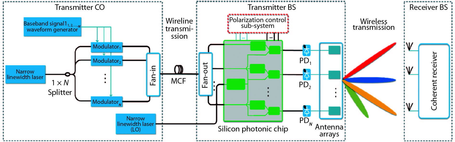
Fig. 1 shows the schematic architecture of a multi-channel fiber-wireless-integration (FWI) transmission system[
![]()
Figure 1.(Color online) The proposed multi-channel FWI system architecture based on the silicon photonic MMW generator.
2.2. Fabricated device and the control sub-system
The micrograph of the fabricated device is shown in Fig. 2(a) with a compact footprint of 1.1 × 2.1 mm2. It implements the SPC for each channel to align the polarization states of the input signal light and that of the LO light. The schematic of the on-chip polarization control units is depicted in Fig. 2(b). The SPC structure was proposed in Ref. [22] to realize an automated polarization receiver in an integrated silicon photonic circuit. At the input port, a polarization splitter and rotator (PSR)[
![]()
Figure 2.(Color online) (a) Micrograph of the fabricated chip. (b) Schematic diagrams of the polarization tuning units. (c) Normalized
where a and b represent the intensities of the two input lights of the first MMI respectively, and a2 + b2 = 1; while ϕ1 and ϕ2 are the initial phase of the two input lights. Normalized PM(Δϕ1, Δϕ2) with different optical power ratios and initial phase differences between the two inputs of the first MMI are numerically calculated and shown in Fig. 2(c). It is observed that PM(Δϕ1, Δϕ2) has two centro-symmetric global minimum points, which means we can reduce the monitored optical power to one of the global minimum points by calculating and setting the proper phase tunings of the two micro-heaters. Then a power-maximized TE polarized signal light at the output port can be obtained. Note that the polarization state of the LO light after vertical coupling is TE-mode due to the TE grating, thus the polarization state of each channel of signal lights is aligned with that of the LO light. Figs. 2(d) and 2(e) show the photograph and schematic of the control sub-system for automated polarization control, respectively. In the control sub-system, each channel of the monitoring lights is sent into a photodetector for optical-to-electrical conversion. Then a trans-impedance amplifier (TIA) is used to amplify the photocurrent signal. The 7 channels of monitored electrical signals are then sampled by analog-to-digital converter (ADC) arrays and sent to a centralized processor. A global minimum-power searching algorithm is then designed and employed in the centralized processer to minimize the monitored optical power at each monitoring port. Different from the polarization control algorithm in Ref. [22], which searches for the minimum power at the feedback port by gradient descent method, the proposed algorithm uses an optimized minimum searching strategy to avoid the affection of the local minima.
Fig. 3 illustrate the pseudo-code of the algorithm, which consists of two minimum-power searching sub-processes in order during one iteration. The minima of PM during the two sub-processes are denoted as PM_min1 and PM_min2, respectively. In sub-process (1), Δϕ1 is tuned to search for PM_min1 with a tuning range of 2π. Then in sub-process (2), Δϕ2 is tuned to further reduce the monitored optical power to approach the global minimum. P1 and P2 are the thermal tuning powers applied on the two micro heaters. By tuning one micro heater over a large phase-shift range at a time instead of switching between the two micro heaters with small steps, the proposed algorithm can effectively prevent the tuning process being trapped into local minima where the monitored signal is buried in noise. Fig. 4 shows this situation, where a local minima exists in the normalizedPM(Δϕ1, Δϕ2) with a 75% to 25% power ratio and a π/2 phase difference between the two inputs of the first MMI. Path (ⅰ) and path (ⅱ) represent the tuning directions of our global minimum-power searching strategy and the gradient descent strategy in Ref. [22], respectively. When the local minima locate near the path from the initial state to one of the global minima, the gradient descent progress will fall into it, while our proposed algorithm would not. In practice, usually one iteration can finely obtain a desired extinction ratio between the output optical power and the monitored optical power. After automated polarization control by the SPC, the signal light is mixed with the LO light by an MMI and then sent to a broadband PD to generate a MMW signal.
![]()
Figure 3.(Color online) Pseudo-code of the global minimum-power searching algorithm.
![]()
Figure 4.(Color online) Progresses of the proposed algorithm and the algorithm in Ref. [
3. Experimental setup and results
To verify the feasibility of the proposed integrated multi-channel MMW signal generator, we perform a proof-of-concept experiment with an experimental setup shown in Fig. 5. At the CO, a CW light at 1550.230 nm from a free-running external cavity laser denoted as ECL1 (Koheras BASIK C15), with a <15-kHz linewidth and 10-dB output optical power is fed into a 25-GHz dual-drive Mach-Zehnder modulator (DDMZM) (T.DKH1.5-40PD-ADC). The DDMZM biased at the quadrature point is driven by two 2-Gb/s pseudo-random bit sequence (PRBS) streams with the same word length of 2 11–1, producing a 2-Gbaud QPSK optical baseband signal. The two electrical baseband signals are generated by an arbitrary waveform generator (AWG) (Keysight M8195A) with a sampling rate of 60-GSa/s and then amplified by two parallel electrical amplifiers (EAs). Note that the baseband signal is resampled to mitigate the sidelobes and therefore minimize the occupied bandwidth. The output optical baseband signal form the DDMZM is divided into 8 channels by a 1 × 8 splitter with ~11-dB single-path insertion loss, and 7 channels are used and fed into different cores of a 2-km 7-core fiber (7CF). The intra-channel crosstalk between adjacent cores is less than –50 dB and the insertion loss of each core is ~ 4.25 dB. Channel decorrelation is carried out by using 7 single-mode fibers (SMFs) with a 2-m interval to ensure that the optical baseband signals in different cores of the 7CF are totally uncorrelated[
![]()
Figure 5.(Color online) Experimental setup of the multi-channel MMW signals generation base on the proposed silicon photonic MMW generator.
![]()
Figure 6.(Color online) On-chip automated polarization-tuning progresses of the 7-channel signal lights.
After the automated polarization tuning for each channel, the signal light and the LO light are combined by the MMI at the output port and coupled out of the chip by vertical coupling. All the vertical coupling ports are connected to a fiber array coupler. The output signal light of one tested channel is then amplified by an EDFA, filtered by an optical bandpass filter (BPF) with a 1-nm bandwidth and detected by a 40-GHz PD (XPDV2120R) to generate a ~28-GHz MMW signal. Before the PD, an optical spectrum analyzer (OSA) (APEX 2040C) with a 1.12-pm resolution is used to record the optical spectrum of the mixed signal, so the powers of the two signals are approximately known. To match the powers of the two lights, the amplification gain of the second EDFA can be adjusted such that the power of the signal light equals to that of the LO light, based on the real-time measurements of the OSA. At the output of the PD, we sample the MMW signal by an 80-GSa/s DSO (LeCroy 10-36Zi-A) and demodulate the baseband QPSK data by offline digital signal processing (DSP), including carrier recovery, down-conversion, symbol synchronization, and signal-to-noise ratio (SNR) measurement. Note that a 28-GHz RF source can perform the demodulation and significantly lower the requirement of the sampling rate. Fig. 7(a) shows the waveforms and the demodulated constellation diagrams of the generated 7-channel QPSK MMW signals. The optical spectrum and the electrical spectrum of channel 1 before and after heterodyne beating are illustrated in Figs. 7(b) and 7(c), respectively. The other channels show similar optical and electrical spectra. Fig. 7(d) gives the SNR performances of the 7 channels of demodulated QPSK signals, which is calculated by the following equation[
![]()
Figure 7.(Color online) (a) Waveforms and the demodulated constellation diagrams of the generated 7-channel QPSK MMW signals. (b) Optical spectrum of channel-1 of the MMW signal before the heterodyne beating. (c) Electrical spectrum of channel-1 of the MMW signal after the heterodyne beating. (d) Measured SNRs of the 7 channels of demodulated QPSK signal.
where N is the symbol number, Ik and Qk represent in-phase amplitude and quadrature amplitude of the kth reference QPSK symbol, respectively, and Xk, Yk are the in-phase amplitude and quadrature amplitude of the kth received QPSK symbol, respectively.
4. Conclusion
In summary, we have proposed a silicon PIC scheme to generate multi-channel MMW signals for large-scale antenna array systems. We have experimentally demonstrated a FWI system, with a 2-km 7CF used as fronthaul transmission of different optical baseband signals, and 7 channels of 28-GHz MMW carrying 4-Gb/s QPSK signals generated in the BS. The MMW signals are demodulated with the best SNR of 17.6 dB. Automated silicon polarization controllers are also implemented with ~7-ms tuning time and ~27-dB extinction ratio.
Acknowledgements
This work was supported by the National Key R&D Program of China under Grant 2016YFB0402501; in part by the Natural Science Foundation of China under grant 61605112, and Open Fund of IPOC under grant BUPT.
References
[1] M Agiwal, A Roy, N Saxena. Next generation 5G wireless networks: A comprehensive survey. IEEE Commun Surv Tut, 18, 1617(2016).
[2] S F Han, C L I, Z K Xu et al. Large-scale antenna systems with hybrid analog and digital beamforming for millimeter wave 5G. IEEE Commun Mag, 53, 186(2015).
[3] Z Pi, F Khan. An introduction to millimeter-wave mobile broadband systems. IEEE Commun Mag, 49, 101(2011).
[4] A I Sulyman, A T Nassar, M K Samimi et al. Radio propagation path loss models for 5G cellular networks in the 28 GHz and 38 GHz millimeter-wave bands. IEEE Commun Mag, 52, 78(2014).
[5] W Roh, J Y Ji-Yun Seol, J Park et al. Millimeter-wave beamforming as an enabling technology for 5G cellular communications: Theoretical feasibility and prototype results. IEEE Commun Mag, 52, 106(2014).
[6] T S Rappaport. Millimeter wave mobile communications for 5G cellular: It will work!. IEEE Access, 1, 335(2013).
[7] R W Heath. An overview of signal processing techniques for millimeter wave MIMO systems. IEEE J Sel Top Signal Process, 10, 436(2016).
[8] X Gao, L Dai, A M Sayeed. Low RF-complexity technologies to enable millimeter-wave MIMO with large antenna array for 5G wireless communications. IEEE Commun Mag, 56, 211(2018).
[9] G Rebeiz. Millimeter-wave large-scale phased-arrays for 5G systems. Microwave Symposium (IMS), IEEE MTT-S International, 1(2015).
[10] X Gao. Energy-efficient hybrid analog and digital precoding for mm-Wave MIMO systems with large antenna arrays. IEEE J Sel Areas Commun, 34, 998(2016).
[11] M Li. Harnessing optical forces in integrated photonic circuits. Nature, 456, 480(2008).
[12] D Marpaung. Integrated microwave photonics. Laser Photonics Rev, 7, 506(2013).
[13] W Zhang, J Yao. Silicon-based integrated microwave photonics. IEEE J Quantum Electron, 52, 1(2016).
[14] R Guzmán, G Carpintero, C Gordon et al. Millimeter-wave signal generation for a wireless transmission system based on on-chip photonic integrated circuit structures. Opt Lett, 41, 4843(2016).
[15] F Amato, G Serafino, P Ghelfi. Ultra-fast beam steering of a phased-array antenna based on packaged photonic integrated circuits. IEEE European Conference on Optical Communication (ECOC), Tu3H(2018).
[16] G Carpintero. Microwave photonic integrated circuits for millimeter-wave wireless communications. IEEE/OSA J Lightw Technol, 32, 3495(2014).
[17] G Carpintero. 95 GHz millimeter wave signal generation using an arrayed waveguide grating dual wavelength semiconductor laser. Opt Lett, 37, 3657(2012).
[18] J Yao. Photonic integrated circuits for microwave signal generation and processing. Conference on Lasers and Electro-Optics (CLEO), JTh4D.1(2018).
[19] M H Khan. Ultrabroad-bandwidth arbitrary radiofrequency waveform generation with a silicon photonic chip-based spectral shaper. Nat Photon, 4, 117(2010).
[20] J Yao. Microwave photonics. IEEE/OSA J Lightw Technol, 27, 314(2009).
[21] R Y Cao, Y He, J P Yao. Integrated multi-channel millimeter wave photonic generation based on a silicon chip with automated polarization control. IEEE European Conference on Optical Communication (ECOC), We2.43(2018).
[22] M L Ma, K Murray, M Y Ye et al. Silicon photonic polarization receiver with automated stabilization for arbitrary input polarizations. Conference on Lasers and Electro-Optics (CLEO), STu4G.8(2016).
[23] M Zhu, L Zhang, J Wang et al. Radio-over-fiber access architecture for integrated broadband wireless services. IEEE/OSA J Lightw Technol, 31, 3614(2013).
[24] A Macho. Next-generation optical fronthaul systems using multicore fiber media. IEEE/OSA J Lightw Technol, 34, 4819(2016).
[25] A Kanno, P T Dat, T Kuri et al. Evaluation of frequency fluctuation in fiber-wireless link with direct IQ down-converter. IEEE European Conference on Optical Communication (ECOC), We.3.6.3(2017).
[26] K Tan. Ultra-broadband fabrication-tolerant polarization splitter and rotator. Optical Fiber Communication Conference, Th1G.7(2017).
[27] A Yariv. Critical coupling and its control in optical waveguide-ring resonator systems. IEEE Photon Technol Lett, 14, 483(2002).
[28] L Luo. WDM-compatible mode-division multiplexing on a silicon chip. Nat Commun, 5, 3069(2014).
[29] Q Zhu et al. Wide-range automated wavelength calibration over a full FSR in a dual-ring based silicon photonic switch. Optical Fiber Communication Conference (OFC), Th3C.1(2018).
[30] N S Bergano, F W Kerfoot, C R Davidsion. Margin measurements in optical amplifier system. IEEE Photon Technol Lett, 5, 304(1993).

Set citation alerts for the article
Please enter your email address
© Copyright 2018-2021 | Chinese Laser Press. All Rights Reserved 沪ICP备15018463号-20