
Minkyu Kim, Min-Hyeong Kim, Youngkwan Jo, Hyun-Kyu Kim, Stefan Lischke, Christian Mai, Lars Zimmermann, Woo-Young Choi, "Silicon electronic–photonic integrated 25 Gb/s ring modulator transmitter with a built-in temperature controller," Photonics Res. 9, 507 (2021)
- Photonics Research
- Vol. 9, Issue 4, 507 (2021)
Abstract
1. INTRODUCTION
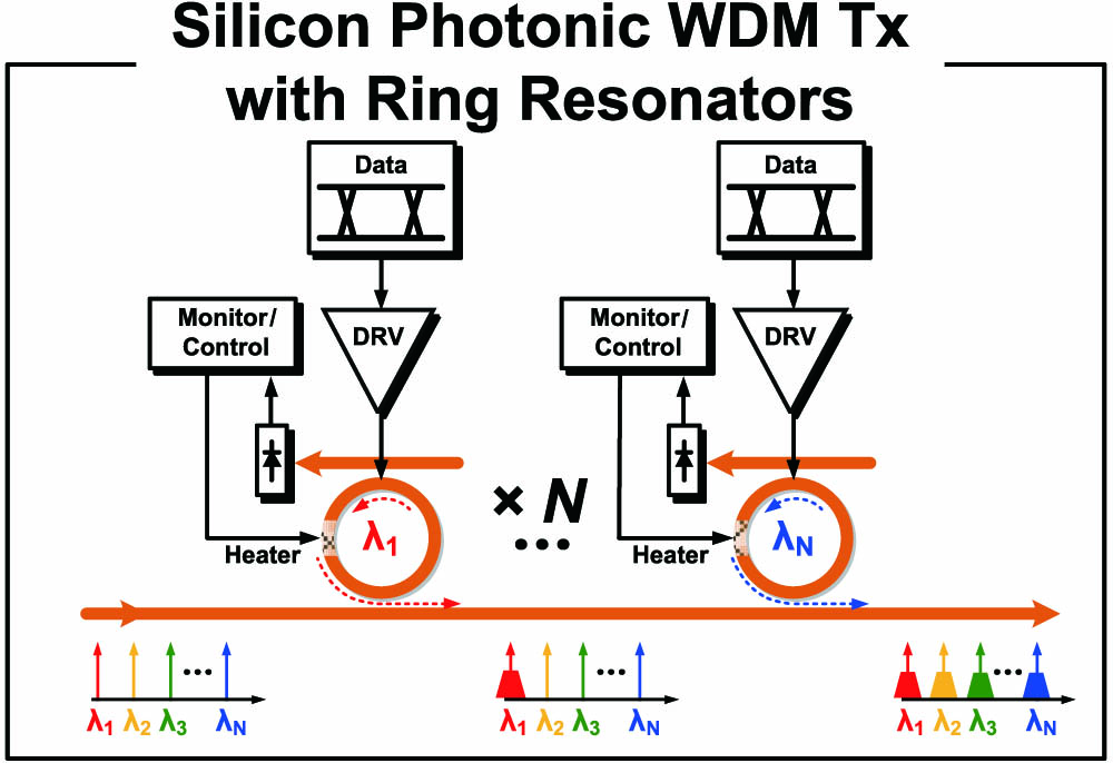
Figure 1.Block diagram of the silicon photonic WDM transmitter with ring resonators.
![]()
Figure 2.Measured transmission curves and 25 Gb/s eye diagrams for different temperatures.
To alleviate the problems discussed above, we have previously reported a custom-designed temperature control IC with which the optimal temperature for the RM OMA is automatically determined in the calibration mode and is stably maintained in the lock mode with a 1-bit dithering technique [17]. This approach, however, requires continuous OMA monitoring in the lock mode, resulting in increased power consumption. In this paper, we present what we believe, to the best of our knowledge, is a new approach in which the OMA monitoring block is used only in the calibration mode. This is achieved using an on-chip temperature sensor [19]. With this, the controller can determine and remember the optimal RM temperature in the calibration mode, and maintain this temperature in the lock mode. In this paper, we explain how our temperature control technique works and provide measurement results based on a 25 Gb/s Si photonic transmitter IC realized on the photonic BiCMOS technology platform [20], which contains monolithically integrated photonic and electronic components.
This paper is organized in four sections. In Section 2, we describe the details of our monolithically integrated Si photonic transmitter along with explanations for the temperature control algorithm. In Section 3, the measurement results for our transmitter are given. Finally, Section 4 concludes the paper. The initial results of this work were reported in Ref. [21], but in this paper, we provide significantly more detailed explanations for our transmitter and the temperature control algorithm is given. Furthermore, the experimental results that verify the stable operation of our transmitter against the larger temperature stress range (from 5°C to 15°C) are presented.
2. RM TRANSMITTER WITH TC CIRCUIT
![]()
Figure 3.(a) Block diagram and (b) fabricated chip photo of the monolithic silicon photonic transmitter with a temperature controller.
![]()
Figure 4.Schematic of the RM driver circuits.
The RM has 12 μm radius and is made up of 500 nm wide waveguides implemented on the standard Si photonic SOI structure. An optical drop port is added to the RM so that OMA can be directly monitored with an integrated Ge PD, as shown in Fig. 3(a). An N-doped Si heater is placed within the ring waveguide, which can change the RM temperature up to 40% of its 8.293 nm free spectral range (FSR). PN-junction-based temperature sensors are placed above and below the RM, which provide voltage signals representing the RM temperature.
Sign up for Photonics Research TOC. Get the latest issue of Photonics Research delivered right to you!Sign up now
![]()
Figure 5.Schematic of the OMA monitor block.
![]()
Figure 6.Schematic of the temperature sensor ADC.
![]()
Figure 7.Timing diagram for the temperature control operation.
In the lock mode, the heater voltage is set to the value determined to produce the maximum OMA in the calibration mode. Then, to maintain the maximum OMA against any temperature perturbation, a PID control is applied to the heater voltage so that the optimum RM temperature is maintained. The OMA monitor block is turned off in the lock mode so that power can be saved. The on-chip digital controller is implemented by synthesis based on a 0.25 μm CMOS standard library provided by the IHP Photonic BiCMOS technology and is composed of more than 2000 transistors.
![]()
Figure 8.Simulation results for the temperature control operation with Verilog-A behavior models.
3. MEASUREMENT RESULTS
![]()
Figure 9.(a) Photo and (b) block diagram of the measurement setup.
![]()
Figure 10.Measured transmission curve of the RM with different on-chip heater powers.
![]()
Figure 11.(a) Measured
![]()
Figure 12.Measurement results for heater voltage (
![]()
Figure 13.Measurement results in the lock mode with thermal stress showing (a) heater voltage (
Table 1 compares the performance of our transmitter IC with recently reported RM temperature control ICs. As can be seen in the table, only in Ref. [16] and the present work, the temperature controller can determine the RM optimal temperature without any external reference and monolithic integration is achieved. The power consumption reported in Ref. [16] is much smaller than our result, which is due to the much advanced SOI CMOS technology used in Ref. [16], not the temperature control algorithm employed. It should also be noted that our temperature control scheme does not depend on the data rate as schemes like in Ref. [15].
Performance Comparison for Silicon Photonic Transmitters with Ring Modulators and Temperature Controllers
| Process | 130 nm SOI SiPh + 65 nm CMOS | 100 nm SOI SiPh + 65 nm CMOS | SiPh + 28 nm CMOS | 130 nm SOI SiPh + 40 nm CMOS | 45 nm CMOS SOI | 0.25 μm BiCMOS | 0.25 μm Photonic BiCMOS |
| Wavelength | 1550 nm | 1310 nm | 1310 nm | 1550 nm | 1180 nm | 1550 nm | 1550 nm |
| Data Rate | 25 Gb/s | 10 Gb/s | 112 Gb/s | 2 Gb/s | 5 Gb/s | 25 Gb/s | 25 Gb/s |
| Driver Integration | Yes (Wire-bonded) | Yes (3D face-to-face) | Yes (3D face-to-face) | Yes (Wire-bonded) | Yes (Monolithic) | No | Yes (Monolithic) |
| Controller Integration | No (Off-chip PD) | Yes (3D face-to-face) | Yes (3D face-to-face) | No (Off-chip DAC) | Yes (Monolithic) | No (Off-chip PD) | Yes (Monolithic) |
| Scheme | Average power | Analog closed-loop w/digital reconfig. | Normalized average power stabilization | OMA monitor w/slope-quantization | Bit-statistics | OMA monitor with power detector & without step approach | OMA monitor with temperature sensing & PID control |
| Manual Reference Setting | Yes | Yes | Yes | No | No | No | No |
| Resonance Wavelength Tuning Range | N/A | N/A | Not reported (50 mW power dissipation) | 5 nm | 2.5 nm | 0.55 nm | 3.27 nm |
| Temp. Controller Power | 0.17 mW | 0.15 mW | Not reported | 2.9 mW | 0.72 mW | 3.91 mW | 3.325 mW |
Excluding heater power
4. CONCLUSION
We present a fully integrated Si photonic transmitter containing a high-speed RM with an on-chip heater and a temperature sensor, a monitor Ge PD, and analog and digital temperature controllers. With two-step calibration and lock mode operations, our transmitter can automatically determine the temperature at which the RM has the maximum OMA and maintain this condition against any temperature fluctuation. Our temperature control scheme is energy efficient and does not depend on the details of RM data rates. With complete monolithic integration of photonic and electronic components achieved with the photonic BiCMOS technology, our transmitter can provide the reduced transmitter size as well as the smaller I/O pin numbers. We also believe that our approach based on photonic and electronic integration can be applied to other photonic devices that require temperature control for best performance.
Acknowledgment
Acknowledgment. The authors thank the IC Design Education Center (IDEC) for EDA tool support.
References
[10] R. Enne, M. Hofbauer, N. Zecevic, B. Goll, H. Zimmermann. Integrated analogue-digital control circuit for photonic switch matrices. Electron. Lett., 52, 1045-1047(2016).


Set citation alerts for the article
Please enter your email address

© Copyright 2018-2021 | Chinese Laser Press. All Rights Reserved 沪ICP备15018463号-20