• Journal of Inorganic Materials
  • Vol. 37, Issue 3, 278 (2022)
Kai LIU1、2, Ce SUN2, Yusheng SHI3, Jiaming HU2, Qingqing ZHANG2, Yunfei SUN2, Song ZHANG4, Rong TU4, Chunze YAN3, Zhangwei CHEN5, Shangyu HUANG2, and Huajun SUN1、*
Author Affiliations
  • 11. State Key Laboratory of Silicate Materials for Architectures, Wuhan University of Technology, Wuhan 430070, China
  • 22. College of Materials Science and Engineering, Wuhan University of Technology, Wuhan 430070, China
  • 33. State Key Laboratory of Materials Processing and Die & Mould Technology, Huazhong University of Science and Technology, Wuhan, 430074, China
  • 44. State Key Laboratory of Advanced Technology for Materials Synthesis and Processing, Wuhan University of Technology, Wuhan 430070, China
  • 55. Additive Manufacturing Institute, Shenzhen University, Shenzhen 518060, China
  • show less
    DOI: 10.15541/jim20210599 Cite this Article
    Kai LIU, Ce SUN, Yusheng SHI, Jiaming HU, Qingqing ZHANG, Yunfei SUN, Song ZHANG, Rong TU, Chunze YAN, Zhangwei CHEN, Shangyu HUANG, Huajun SUN. Current Status and Prospect of Additive Manufacturing Piezoceramics[J]. Journal of Inorganic Materials, 2022, 37(3): 278 Copy Citation Text show less
    Papers published on additive manufacturing of piezoceramics (data from Web of Science)
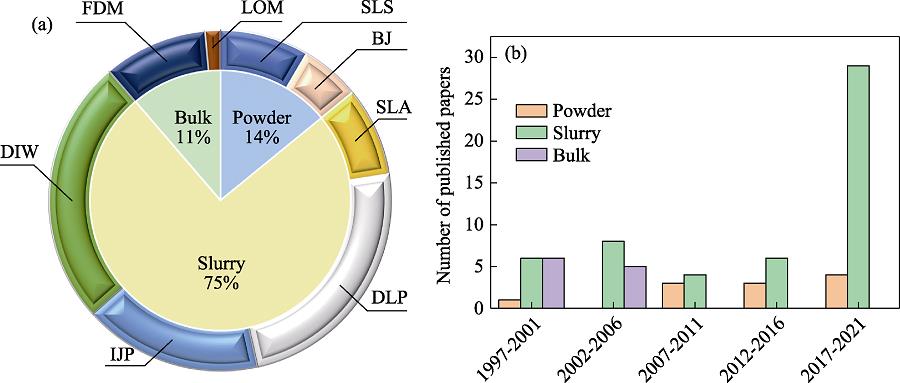
    1. Papers published on additive manufacturing of piezoceramics (data from Web of Science)
    Piezoceramic with lattice structure formed by Binder Jetting[18]
    2. Piezoceramic with lattice structure formed by Binder Jetting[18]
    Schematic diagram of layered exposure strategy (a) and micro-topography photo of sintered part[32] (b), photo of precursor body fabricated by Digital Light Processing (c), photos of BTO sample after sintering[35] (d), photos of PZT ceramic microarrays fabricated by Binder Jetting[37] (e)
    3. Schematic diagram of layered exposure strategy (a) and micro-topography photo of sintered part[32] (b), photo of precursor body fabricated by Digital Light Processing (c), photos of BTO sample after sintering[35] (d), photos of PZT ceramic microarrays fabricated by Binder Jetting[37] (e)
    Micro-morphology photos of the PZT ceramics sintered at different temperatures (a) and photos of sintered PZT ceramics fabricated by Direct Ink Writing (b)[41], and cross-section photo of gradient piezoelectric ceramics fabricated by Fused Deposition Modeling (c)[51,52]
    4. Micro-morphology photos of the PZT ceramics sintered at different temperatures (a) and photos of sintered PZT ceramics fabricated by Direct Ink Writing (b)[41], and cross-section photo of gradient piezoelectric ceramics fabricated by Fused Deposition Modeling (c)[51,52]
    Photos of BTO/HA piezoelectric ceramics fabricated by Binder Jetting (a) and SEM images of the sample after 24 h MC3T3-E1 cells incubation (b)[70], piezoelectric ceramics and piezoelectric composite materials fabricated by Digital Light Processing (c), the underwater acoustic testing device and the output voltage of the hydrophone under different acoustic excitation frequencies (d) [32], the photo of CPE sample (e) and the packaged ultrasound scanning equipment (f), and pig eye ultrasound imaging results (g)[74]
    5. Photos of BTO/HA piezoelectric ceramics fabricated by Binder Jetting (a) and SEM images of the sample after 24 h MC3T3-E1 cells incubation (b)[70], piezoelectric ceramics and piezoelectric composite materials fabricated by Digital Light Processing (c), the underwater acoustic testing device and the output voltage of the hydrophone under different acoustic excitation frequencies (d) [32], the photo of CPE sample (e) and the packaged ultrasound scanning equipment (f), and pig eye ultrasound imaging results (g)[74]
    Schematic (a) and picture (b) of piezoelectric sensor device[31]
    6. Schematic (a) and picture (b) of piezoelectric sensor device[31]
    MaterialsProcessDensity/(g·cm-3) Relative density/%d33/(pC·N-1) Relative dielectric constant (εr) Dielectric loss (tan δ) Ref.
    BTOSLS-97-1800-[7]
    PZTSLS450.6---[12]
    PZTLENS-90-4300.05[14]
    BTOBJ-93-94183--[18]
    BTOSLA5.699516327620.016[23]
    BTODIW5.1385.24204.612551-[44]
    PZTDIW(7.21±0.06)94.9678(4132±575)(3.4±1%)[45]
    BTODIW5.42902002200-[46]
    BTODIW-89.973502576-[47]
    PLZTDIW-984811986-[48]
    BCZTDIW-9310010460.021[49]
    BTODIW-961591900-[50]
    BTOBJ2.2137113(Horizontal) 152.7(Vertical) 581.6(Horizontal) 698(Vertical) -[56]
    KNNSLA4.3296-1800-19000.2-0.3[57]
    PMN-PTDLP7.9897.8620--[58]
    PZTDLP7-34513900.021[59]
    KNNDLP4.099217021500.058[60]
    PZT-5HDLP7.359660028750.029[61]
    BTODLP5.449020019650.017[62]
    PZTIJP-(86±3)-1900.05[63]
    BTODIW3.9365.320047300.033[64]
    BTODIW-98195--[65]
    BTODIW-97.8-533-[66]
    BTODIW5.669442043800.02[67]
    PZTFDM7.7-66433400.023[68]
    Table 1. Comparison of properties of piezoceramics formed by additive manufacturing
    Kai LIU, Ce SUN, Yusheng SHI, Jiaming HU, Qingqing ZHANG, Yunfei SUN, Song ZHANG, Rong TU, Chunze YAN, Zhangwei CHEN, Shangyu HUANG, Huajun SUN. Current Status and Prospect of Additive Manufacturing Piezoceramics[J]. Journal of Inorganic Materials, 2022, 37(3): 278
    Download Citation