
Chen Xu, Changda Zheng, Xiaoming Wu, Shuan Pan, Xingan Jiang, Junlin Liu, Fengyi Jiang. Effects of V-pits covering layer position on the optoelectronic performance of InGaN green LEDs[J]. Journal of Semiconductors, 2019, 40(5): 052801
- Journal of Semiconductors
- Vol. 40, Issue 5, 052801 (2019)
Abstract
1. Introduction
GaN, which is an important semiconductor material, and its related alloys (AlInGaN) have recently attracted wide attention[
Since these V-pits are generated from the dislocation of stress-release layer, laying through the multi-quantum wells (MQWs) region[
2. Experiments
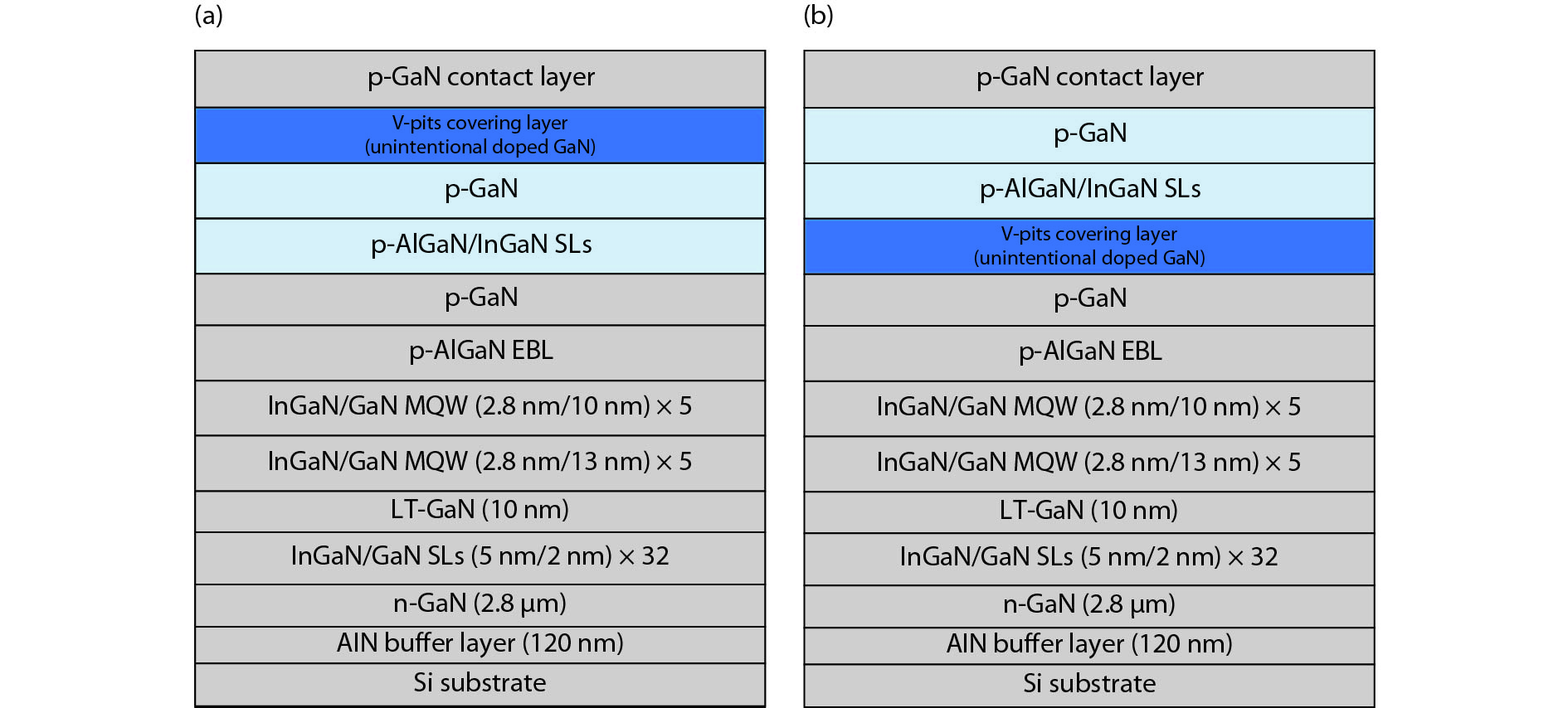
The investigated samples were grown on 2-inch silicon (111) substrates by a Thomas Swan close-coupled showerhead metal organic chemical vapor deposition (MOCVD) system. To investigate the effect of the VCL on the hole injection, we have grown two samples with different position of the VCL. As shown in Fig. 1(a), the epitaxial structure of sample A consists of a 120-nm-thick AlN buffer layer, a 2.8-μm-thick Si-doped (5 × 1018 cm−3) n-GaN, a 32 period superlattice layer, and a 10-nm-thick low-temperature GaN (LT-GaN). The active region consists of two kinds of MQW, the five pairs of QWs closed to the n-type layer were 2.8 nm-InGaN/13 nm-GaN and the five pairs of QWs closed to p-type layer were 2.8 nm-InGaN/10 nm-GaN[
![]()
Figure 1.(Color online) Schematic epitaxial structures of two samples with different position of V-pits covering layer.
3. Results and discussions
The temperature-dependent EQEs as a function of current density are shown in Fig. 2. The EQEs of two samples are almost identical at room temperature. However, when the temperature drops from 300 to100 K, sample B has a higher EQE in region Ⅰ but a lower EQE in region Ⅱ. Since the EQE is mainly influenced by the hole injection efficiency at region Ⅰ [
![]()
Figure 2.(Color online) The temperature-dependent EQE as a function of currents at (a) 300 K, (b) 200 K, (c) 150 K, (d) 100 K, respectively.
The STEM images of the epitaxial structure with V-pits in two samples are shown in Fig. 3. For convenience, we define the two heavily doped p-GaN layers and the p-AlGaN/InGaN SL in sample A as a hole injection layer (HIL), the single heavily Mg-doped p-GaN layer in sample B as a hole injection layer 1 (HIL1), the p-AlGaN/InGaN SL and another heavily Mg-doped p-GaN layer grown subsequently as a hole injection layer 2 (HIL2). As a result of the different position of VCL, the V-pits in sample A contain the entire HIL grown subsequently, as shown in Fig. 3(a), but only contain a single p-GaN layers in sample B and are then filled with the unintentional-doped VCL, as shown in Fig. 3(b). This means that the hole concentration in V-pits of sample A is higher than that of sample B. Moreover, since the resistivity of the VCL in V-pits is higher than that of the VCL in the c-plane due to the special inverted pyramid structure, the holes in sample B generated from the HIL2 above the V-pits are easier to flow through the c-plane rather than drop directly into the V-pits. The effect of these factors on hole injection efficiency may not obvious at room temperature due the sufficient hole concentration. However, when the hole concentration decreases dramatically due to the acceptors freezing out with temperature decrease[
![]()
Figure 3.(Color online) The STEM image of two samples with V-pits structure.
The current–voltage curves of two samples at various temperatures are demonstrated in Fig. 4. Sample B has a higher operating voltage at room temperature and the degree of voltage difference between two samples is amplified with the temperature drop. The V-pits can effectively decrease the operating voltage due to the improved injection of holes via the sidewall of V-pits[
![]()
Figure 4.(Color online) Current–voltage curves in linear scale of two samples at (a) 300 K, (b) 200 K, (c) 150 K, (d) 100 K, respectively.
Fig. 5 shows the EL spectra of the two experimental samples at various injection currents at 100 K. P1 and P2 are emitted from the QWs closer to p-GaN and the QWs closer to n-GaN, respectively. P3 is emitted from the sidewalls QWs. It is worth noting that P3 in sample B emerges at a lower current density and is more manifested than that in sample A. This indicates that the holes in sample B injected into the sidewall QWs take part in radiative recombination with electrons more easily than that in sample A. The observed emission of P2 from the deeper QWs near the n-GaN in sample B demonstrates that the holes in sample B could be transported further than those in sample A. Based on the correlation analysis of structural characteristics and the I–V characteristics of two samples mentioned above, these phenomena should be correlated with the increased kinetic energy of holes, which changes the transport paths of holes in sample B. For a better understanding of the changes in the transport paths, Fig. 6 schematically display the possible transport paths of holes in two samples with different VCL positions. At room temperature, most of the holes in sample B were normally injected into MQWs via path 1 and path 2 due to the high resistance in the V-pits. However, when the temperature decreases, the higher operating voltage of sample B can speed up the holes. This gives the holes enough kinetic energy to inject into the sidewall of V-pits via path 3. Hence, when most of the holes injected into sidewall QWs of V-pits in sample A are diffused into the c-plane QWs via the path 2 provided by V-pits[
![]()
Figure 5.(Color online) The EL spectra of two experimental samples at various injection currents at 100 K.
![]()
Figure 6.(Color online) Schematic diagram of the potential transport paths of holes in two samples with different position of VCL.
4. Conclusion
In summary, the effect of VCL position on the optoelectronic performance of high-efficiency green LEDs has been studied. It was found that the earlier covering of V-pits will hinder the hole injection via the sidewall of V-pits, and then result in a higher EQE at low current density and an earlier droop with the increasing current density. Meanwhile, the reduced proportion of hole injection via the sidewall of V-pits also results in a higher operating voltage at room temperature and a dramatic increase in voltage as the temperature decreases. The higher operating voltage gives the hole injected via the sidewall of V-pits higher kinetic energy. This then leads to the emissions of sidewall QWs and deeper QWs near to n-type layer. Finally, the results of this investigation show that the VCL should be properly doped to provide suitable hole concentration and operating voltage.
Acknowledgements
This work was supported by the State Key Program of the National Science Foundation of China (Grant No. 61334001), the National Key R&D Program of China (Grant Nos. 2016YFB0400600 and 2016YFB0400601), and Development Program of Jiangxi province (Grant No. 20165ABC28007 and No. 20182ABC28003).
References
[1] G Deng, Y Zhang, Y Yu et al. Significantly reduced in-plane tensile stress of GaN films grown on SiC substrates by using graded AlGaN buffer and SiN
[2] L Yan, Y Zhang, X Han et al. Polarization-induced hole doping in N-polar III-nitride LED grown by metalorganic chemical vapor deposition. Appl Phys Lett, 112, 182104(2018).
[3] G Deng, Y Zhang, Y Yu et al. Significantly improved surface morphology of N-polar GaN film grown on SiC substrate by the optimization of V/III ratio. Appl Phys Lett, 112, 151607(2018).
[4] G Deng, Y Zhang, Y Yu et al. Study on the structural, optical, and electrical properties of the yellow light-emitting diode grown on free-standing (0001) GaN substrate. Superlattices Microstruct, 116, 1(2018).
[5] L Junlin, Z Jianli, W Guangxu et al. Status of GaN-based green light-emitting diodes. Chin Phys B, 24, 39(2015).
[6] M H Crawford. LEDs for solid-state lighting: performance challenges and recent advances. IEEE J Sel Top Quantum Electron, 15, 1028(2009).
[7] J Piprek. Origin of InGaN/GaN light-emitting diode efficiency improvements using tunnel-junction-cascaded active regions. Appl Phys Lett, 104, 2217(2014).
[8] A Hangleiter, F Hitzel, C Netzel et al. Suppression of nonradiative recombination by V-shaped pits in GaInN/GaN quantum wells produces a large increase in the light emission efficiency. Phys Rev Lett, 95, 127402(2005).
[9] Z Quan, L Wang, C Zheng et al. Roles of V-shaped pits on the improvement of quantum efficiency in InGaN/GaN multiple quantum well light-emitting diodes. J Appl Phys, 116, A779(2014).
[10] Y Li, F Yun, X Su et al. Deep hole injection assisted by large V-shape pits in InGaN/GaN multiple-quantum-wells blue light-emitting diodes. J Appl Phys, 116, 253512(2014).
[11] S Zhou, X Liu. Effect of V-pits embedded InGaN/GaN superlattices on optical and electrical properties of GaN-based green light-emitting diodes. Phys Status Solidi Appl Res, 214, 1770125(2016).
[12] H Takahashi, A Ito, T Tanaka et al. Effect of intentionally formed `V-defects' on the emission efficiency of GaInN single. Jpn Soc Appl Phys, 39, 569(2000).
[13] S M Ting, J C Ramer, D I Florescu et al. Morphological evolution of InGaN/GaN quantum-well heterostructures grown by metalorganic chemical vapor deposition. J Appl Phys, 94, 1461(2003).
[14] L C Le, D G Zhao, D S Jiang et al. Effect of V-defects on the performance deterioration of InGaN/GaN multiple-quantum-well light-emitting diodes with varying barrier layer thickness. J Appl Phys, 114, 143706(2013).
[15] Q Lv, J Liu, C Mo et al. Realization of highly efficient InGaN green LEDs with sandwich-like multiple quantum well structure: role of enhanced interwell carrier transport. ACS Photonics, 6, 130(2018).
[16] G Wang, X Tao, J Liu et al. Temperature-dependent electroluminescence from InGaN/GaN green light-emitting diodes on silicon with different quantum-well structures. Semicond Sci Technol, 30, 15018(2014).
[17] X Wu, J Liu, Z Quan et al. Electroluminescence from the sidewall quantum wells in the V-shaped pits of InGaN light emitting diodes. Appl Phys Lett, 104, 1634(2014).
[18] J Kim, Y Tak, J Kim et al. Analysis of forward tunneling current in InGaN/GaN multiple quantum well light-emitting diodes grown on Si (111) substrate. J Appl Phys, 114, 231107(2013).
[19] P Kozodoy, H Xing, S P Denbaars et al. Heavy doping effects in Mg-doped GaN. J Appl Phys, 87, 1832(2000).
[20] W Xiaoming. Study on the luminescence properties of V-pits-containing GaN based blue LEDs on Si substrates. Nanchang University(2014).
[21] E F Schubert, T Gessmann. Light emitting diodes. Encylopedia of Condensed Matter Physics, 102(2005).


Set citation alerts for the article
Please enter your email address

© Copyright 2018-2021 | Chinese Laser Press. All Rights Reserved 沪ICP备15018463号-20