1SZU-NUS Collaborative Center and International Collaborative Laboratory of 2D Materials for Optoelectronic Science & Technology of Ministry of Education, College of Optoelectronic Engineering, Shenzhen University, Shenzhen 518060, China
2Engineering Technology Research Center for 2D Material Information Function Devices and Systems of Guangdong Province, College of Optoelectronic Engineering, Shenzhen University, Shenzhen 518060, China
As a kind of two-dimensional transition metal dichalcogenide material, tungsten diselenide () has attracted increasing attention, owing to its gapped electronic structure, relatively high carrier mobility, and valley pseudospin, all of which show its valuable nonlinear optical properties. There are few studies on the nonlinear optical properties of and correlation with its electronic structure. In this paper, the effects of spatial self-phase modulation (SSPM) and distortion influence of ethanol suspensions are systematically studied, namely, the nonlinear refractive index and third-order nonlinear optical effect. We obtained the dispersions SSPM distortion formation mechanism, and through it, we calculated the nonlinear refractive index , nonlinear susceptibility , and their wavelength dependence under the excitation of 457 nm, 532 nm, and 671 nm lasers. Moreover, by use of its strong and broadband nonlinear optical response, all-optical switching of two different laser beams due to spatial cross-phase modulation has been realized experimentally. Our results are useful for future optical devices, such as all-optical switching and all-optical information conversion.
1. INTRODUCTION
From the early discovery of two-dimensional (2D) material graphene, many endeavors have concentrated on developing 2D materials that exceed graphene, such as transition metal dichalcogenides (TMDCs) [1–3]. TMDCs consist of two layers of sulfide atoms and a sandwiched layer of metal atoms [4], forming an atomic tri-layer chemical formula shaped like . The tri-layer films are superposed by weak van der Waals interactions to form a 3D entity [5]. According to the combination of the sulfur family (S, Te, Se) and transition metals (Mo, Nb, Re, W, Ni, V) [6], TMDCs produce over 40 different kinds. TMDCs are likely to be integral parts of future electric optical devices, such as all-electric optical switches that act as metals, semi-metals, or semiconductors according to the selection of transition metals [7].
Tungsten diselenide () is drawing more and more interest because of its comparatively high carrier mobility, interstitial electronic structure, and valley pseudospin, which all denote diverting nonlinear optical properties of this TMDC material [8,9]. In 1970, ultrathin film comprising only two layers was favorably prepared by mechanical stripping, and the thickness effect of exciton transition was revealed [10]. is a layered semiconductor with a hexagonal crystalline structure and an indirect bandgap of 1.35 eV. The optical properties of transfer mainly from two direct excitons at 1.71 eV and 2.30 eV, called A and B excitons, severally [11,12]. has been broadly used in photo-electron chemical solar cells as an electrode [13] and hydrogen evolution [14], according to its high absorption coefficients and photo-corrosion resistance in the visible range. In addition, depending on its flexible layered structure and low surface trap density, it is an attractive flexible electronic candidate. Formerly, we have proved that field effect transistors have been obtained at room temperature, and the carrier mobility is equivalent to that of silicon [15]. Recently, has been prepared in many ways, such as solution phase synthesis [16], mechanical exfoliation [17], rapid selenization process [18], and modulated elemental reaction [19].
To comprehend these 2D materials, the nonlinear refractive index and third-order nonlinear susceptibility have been studied by using four-wave mixing, Z-scan, and spatial self-phase modulation (SSPM) [20–23]. The Z-scan mechanism is based upon self-focusing or self-defocusing whose spot is a Gaussian beam, and different from the mechanism of SSPM self-diffraction whose spot is a concentric circle. The SSPM technique has become a useful means for measuring the nonlinear coefficient of 2D materials. In order to estimate the nonlinear refractive index of [24,25], nonlinear characteristic parameters are analyzed by using SSPM in this paper.
Sign up for Photonics Research TOC. Get the latest issue of Photonics Research delivered right to you!Sign up now
Optical switching devices based on 2D materials can be designed using the nonlinear optical effect [26]. Wu et al.[27] exhibited an all-optical switch that relies on dual-color (473 nm and 532 nm) SSPM using in 2015. They created a model at 473 nm (controlled light) by raising the beam intensity to 532 nm (controlling light). The ring numbers and diameters increase at the same time, and the fixed intensity of 473 nm is lower than the threshold. The physical mechanism can be traced back to cross-phase modulation (XPM) [28,29], which refers to a nonlinear phase change of the light field caused by other co-propagating fields [30]. In two or more laser fields, self-phase modulation (SPM) is always accompanied by XPM, which has always been covered in optical fibers [31].
In this paper, the SSPM effect of ethanol suspension is studied. First, the conventional preparation method of and the preparation steps of dispersion in this experiment are briefly described. Then, the characterization method of and the characterization results of this sample are summarized. Then, the apparatus diagram of this experiment is introduced. The images of the SSPM effect taken in multiple bands are also given, and and values of are analyzed and calculated by taking the experiment at wavelengths of 457 nm, 532 nm, and 671 nm lasers. Taking advantage of the advanced optical properties of , we can design a novel nonlinear all-optical switching device combined with the information transmission system based on spatial cross-phase modulation (SXPM).
2. PREPARATION AND CHARACTERIZATION OF WSe2 NANOPARTICLES
A. Preparation of WSe2 Nanoparticles
2D material ethanol suspensions were produced by the liquid phase stripping method for further experimental investigations. With the mixture of organic solvents, using ultrasound, the interlayer van der Waals force was overcome, and then dispersions were obtained through a centrifugal method removing the block from a single layer, and multilayer and fewer block mixed suspensions. Bulk () and ethanol (, 99.9%) were purchased from Sigma-Aldrich. First, 20 mg was added to 20 mL ethanol, and then the whole solution was treated with bath sonication whose power was set at 300 W for 10 h, and the working temperature of the bath sonication was at controlled around 10°C. After this process, the obtained suspension was centrifuged for 60 min with a rotation rate of 5000 r/min, followed by 12 h natural settling. The upper layer liquid from the last step was centrifuged for 40 min with a rotation rate of 12,000 r/min. The resulting supernatant was composed of a few-layer dispersion used in the following experiments.
B. Characterization of Few-Layer WSe2 Nanoparticles
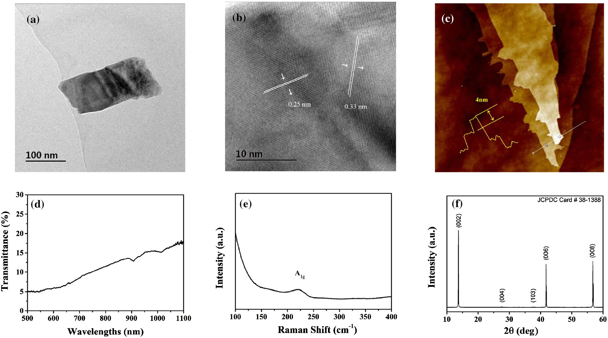
The dispersion solution was dropped onto an ultra-thin copper mesh, and then dried in an arid cabinet, imaged by transmission electron microscopy (TEM), which shows the bedded structure of nanoparticles, as in Fig. 1(a). The image edges are clearly visible, and the folds on the surface are also obvious.
Figure 1.Characterization of nanoparticles after stable storing for two weeks. (a) TEM image, (b) HRTEM image, (c) AFM image, (d) transmittance spectrum, (e) Raman spectrum, and (f) XRD pattern.
The high-resolution TEM (HRTEM) image in Fig. 1(b) shows the 2D honeycomb structure of with a tight arrangement of atoms. The observed spacings of the lattice fringes are 0.329 nm and 0.247 nm, respectively. Atomic force microscopy (AFM) was used to characterize thin film morphology and atom structure; the thin film was made by deposition of dispersion on a silicon wafer, as shown in Fig. 1(c). From thin-film height of 4.1 nm, we also can identify the layer number as about six.
In the transmittance spectrum wavelength from 500 nm to 1100 nm, shown in Fig. 1(d), we can clearly find that the transmissivity of nanoparticles is in the range of 4.87%–17.98% and has two peaks at 907 nm (12.82%) and 1016 nm (15.23%). In Fig. 1(e), Raman spectroscopy is one of the important means to distinguish the 1–10 layers of 2D ultra-thin layered materials. It analyzes the molecular structure of the sample by the principle of changing the frequency of the scattering light when the light is irradiated to the sample. The Raman spectrum of the nanoparticle suspension displays a broad band with peak maximum at [32]. Figure 1(f) gives the X-ray diffraction (XRD) curve of nanoparticles, showing peaks at 13.6°, 27.5°, 37.8°, 41.8°, and 56.7°.
3. RESULTS AND DISCUSSION
A. Scheme of SSPM Experiment
Figure 2 displays a diagrammatic sketch of the SSPM experiment. A wavelength of continuous-wave (CW) laser (while in the following experiment, wavelengths of and were also included) was used as a light source. This laser beam passed the polaroid, focalized after the lens (), and then passed through dispersion, which was filled in a 10 mm thickness quartz cuvette. Distances between the focus point and sample were set as 3.7 cm, 4.8 cm, and 9.2 cm. values were quartz cuvette thickness plus . The CW laser engendered phase-shift passing the dispersion, motivated the SSPM effect, and diverged into diffraction rings. The diffraction ring patterns can be obtained from a black screen suspended behind the sample quartz cuvette, and also can be obtained from a charge-coupled device (CCD, LaserCam HR II 2/3 inch), which was produced by Coherent.
Figure 2.Diagrammatic sketch of the measuring experimental setup.
The nanoparticle dispersion was prepared by the liquid stripping technique. The results show that the diffraction ring pattern experienced rapid deformation when the incident CW laser passed through the dispersion horizontally. Figures 3(a)–3(c) show the corresponding pictures taken by CCD and record all of the SSPM conversion process. From 0 to 0.42 s, after the CW laser passed through the few-layer dispersion, the diffraction pattern started from a small round circle and quickly became a series of complete symmetric concentric rings. From 0.42 s the diffraction rings began to distort rapidly, until at 1.23 s reaching a stable collapsed pattern. The top half of the diffraction ring collapsed toward the center of the pattern, and the bottom half of the ring remained almost an original full round circle and formed a sub-elliptical diffraction ring. The collapse is very obvious in the vertical direction, and in the upper part of the ring, the closer to the outer collapse, the more obvious collapse effect we got.
Figure 3.(a)–(c) Diffraction rings received by a CCD of SSPM transformation; (d) schematic of the distortion for nanoparticle dispersions.
The above phenomenon is called the collapse effect of diffraction rings in SSPM. The collapse effect is very important for studying the variation of the nonlinear refractive index of 2D materials. The change in refractive index for nonlinear materials caused by lasers can be measured by the collapse effect.
B. Collapse Dependent on Light Intensity
In addition to temperature response, collapse distortion also shows obvious regularity with the intensity of light, all of which shows linear variations. The patterns of classical SSPM effect are shown in Figs. 3(a)–3(c); the collapse amplitude of the upper part can be described by angles formed from the sample to pattern. When diffraction rings appear, a series of coaxial cones are formed by a diffractive light path in space. The angle from the axis of the largest cone to the side of the cone is a half-conical angle, i.e., collapse distance , the maximum half diffraction angle is , and maximum diffraction radius is . D is the distance from the sample to the pattern; the values are 8.1 cm, 8.9 cm, and 9.8 cm at the wavelengths of , , and , shown in Fig. 3(d). On the basis of , the relationship can be explained as When the diffraction ring collapses and stabilizes, the maximum half-angle of the diffraction pattern of the first half part is , and the maximum diffraction radius is changed to . If , the relationship can be conveyed as the following equation: The distortion angle and diffraction radius are defined as and ; on the basis of , the relationship between them can be displayed as The distortion angle can be displayed as the next expression [22]: Finally, the relation between the relative variable of the nonlinear refractive index and collapse angle and the maximum half-diffractive angle is obtained by eliminating the maximum half-diffraction angle constant [33]: From diffraction patterns caught by CCD, we obtained the distance from the pattern and got the variation of the distortion angle () and half-cone angle () with the incident intensity change at , , and , as shown in Figs. 4(a) and 4(b).
Figure 4.(a) Variation of the half-cone angle () with incident intensity; (b) variation of the distortion angle () with incident intensity; (c) change in the nonlinear refractive index of after distortion.
Through calculation, we can obtain the change rate of the nonlinear refractive index, as shown in Fig. 4(c). For , intensity from increases to , accomplishing the half-cone angle () from 0.024 mrad to 0.121 mrad, in a nearly linear manner; distortion angle () from 0.020 mrad to 0.037 mrad is also a linear change. and also have the same regular results. This means that the distortion results in a significant change of nonlinear refractive index in the dispersion of several layers nanoparticles.
Therefore, in the measurement, through the ratio of collapse angle to maximum half-diffraction, can obtain the relative change of the nonlinear refractive index of the dispersion. The results show that the relative change in nonlinear refractive index varies with light intensity. When light intensity increased from to , the change was monotone, from 30.57% to 83.33% at 532 nm. In other words, the larger the incident intensity, the greater the change in nonlinear refractive index and the more obvious the collapse, which is consistent with the observed collapse effect. Light sources at and have got the same regular results.
C. Wavelength Dependence of Third-Order Nonlinear Susceptibility
A light field through nanoparticles can cause a change in refractive index, producing some well-known optical phenomena, for instance, self-phase modulation and self-focusing. According to the nonlinear optical Kerr’s law, when a laser beam passes through a nonlinear optical medium, in this case, nanoparticles, the light intensity will cause the refractive index to change, and the change in refractive index causes the phase movement of the light; the change in refractive index can be explained as follows: where and are the nonlinear and linear refractive indices, and represents the incident intensity. It can be clearly seen from the above equation that the refractive index of the medium is related to the light intensity, and the refractive index of the medium changes with the intensity of light, which is also a significant feature of the optical Kerr effect.
When the laser beam passes through dispersion, the SSPM phenomenon is generated, and the phase shift () is shown as follows: where is the wavelength, is an effective optical propagation length, is the radial position, and is the intensity distribution. The effective thickness of the quartz cuvette can be calculated by [22]where is the Rayleigh length, is the propagation length, and is the thickness of the cuvette. For a Gaussian beam, the phase shift can be satisfied, and is equal to beam radius. The bright and dark rings [22] alternately occur when the phase shift is related to the ring number [34]. After derivation, the nonlinear refractive index of can be written as [35]The third-order nonlinear susceptibility of 2D nonlinear material is defined as . From the slope of the ring number and incident intensity, of nanoparticles can be expressed by The third-order nonlinear susceptibility for monolayer nanoparticles can be obtained by where is the effective amount of the monolayer.
Figure 5 shows the relationship between the diffraction ring number received by CCD and the intensity of different wavelengths at , , and .
Figure 5.Variation of diffraction ring numbers with incident intensity at , , and , respectively.
In Fig. 5, we clearly see the linear relationship between the number of rings and the intensity with a slope of for . After fitting, we yielded the nonlinear refractive index and the third-order nonlinear susceptibility . The distance from the lens to the cuvette is 15.3 cm. The transmission of monolayer , which was got from Refs. [36,37], is 92.93% at the 532 nm wavelength, and for the dispersion sample in this paper the transmission is 4.94%, and then we got the as 41, and as .
Figure 5 shows the variation of diffraction rings for with incident intensity, and the fitting result is and . The length between the lens and cuvette is 14.2 cm for 671 nm. The transmissions of monolayer and dispersion in our research at 671 nm wavelength are 98.81% and 7.38%, respectively. We finally got the as 218, and as .
In addition, Fig. 5 proves the change in diffraction rings with intensity at , and and are acquired by fitting. The distance from the lens to the cuvette is 9.8 cm for the 457 nm laser beams. is 28, and is , which is calculated from the transmissions of monolayer at 89.50% and our sample at 4.28%.
Table 1 give the summary of the relations between optical parameters and wavelengths of different 2D materials [38–40].
It is known that diffraction rings are a result of SSPM related to the local refractive index change caused by a laser. However, there are several competing theories about the origin of refractive index variations. For instance, the thermal lens theory is proposed to describe the change in the refractive index of the medium with the change in temperature resulted from absorbing the laser light [41]. In order to understand the origin of diffraction rings, we investigate the SSPM by a Nd:YAG nanosecond (ns) laser (Beamtech model DAWA-200, 532 nm, 8 ns) with low repetition rate (20 Hz) as a comparison to the results with the CW laser. The results are shown in Fig. 6(b). It is found that the number of rings in the ns laser is nearly half that of the CW laser at the same power. We tuned the repetition rate of the ns laser to 10 Hz; it is found that the number of rings is almost unchanged, indicating the possible electronic origin of SSPM. Moreover, the whole transformation processes of SSPM caught by a white screen are shown in Fig. 6(a). Under the CW laser, the formation of the whole diffraction rings needs 0.42 s, and going to distortion needs 1.23 s. But if we use the ns laser, the formation progress takes only 0.20 s, and distortion progress takes 0.65 s. It is obvious that the intrinsic nonlinear effect from the material plays an important role in the formation of diffraction rings in the low-repetition-rate pulsed laser. However, the thermal lens effects have a significant impact on the formation of diffraction rings using the CW laser. These indicate that both intrinsic nonlinear optics and thermal lens effect may have contributions to the phase modulation under intense CW laser excitation.
Figure 6.(a) Transformation of SSPM. (1)–(3): continuous wave; (4)–(6): ultrafast wave. (b) Variation of diffraction ring numbers with continuous wave and ultrafast wave.
In the experiment, the optical control of light technology based on the SXPM effect with was discussed. This optical switching of nanoparticle dispersion liquid was disposed by using CW 671 nm controlling light (HNL210L) to modulate/manipulate the propagation of the 532 nm controlled light (SPROUT-H-5W). The controlling light and controlled light were placed at equal height passing through the nanoparticle dispersion liquid, which was put in a 2 mm thick quartz cuvette. The intensities of these two lights were changed by attenuation slices, passed a focusing lens, and focused on the center of the quartz cuvette. By increasing the incident intensity of the controlling light, the nonlinear phase in the dispersion liquid could be controlled. Figure 6 shows the schematic diagram of the experimental configuration. After combining the laser beam through the lens and the sample, we can see the diffraction ring behind the white screen. Figure 7 shows the experimental configuration for the all-optical switching, and Figs. 8(b) and 8(c) show the images of the SXPM effect in .
Figure 7.Schematic of the experimental configuration for all-optical switching.
Figure 8.(a) Results obtained by using a relatively strong laser beam to control the other laser beam with relatively weak power at ; (b), (c) images obtained from white screen.
In the beginning, laser intensity of controlled light at 671 nm is adjusted below the diffraction ring excitation threshold whose intensity is set at shown as a Gauss laser spot, which indicates that there is no nonlinear optical effect at this incident intensity. Later, the controlling light at 532 nm is used to excite the diffraction ring of controlled light at 671 nm. Slowly increasing the incident intensity of the controlling light to while the controlled light was kept at an intensity of , the diffraction rings of both the controlling light and controlled light in the transmitted spots can be surveyed. In addition, the diffraction ring numbers of the 532 nm and 671 nm beams rise with the increasing of the incident intensity of the 532 nm controlled light.
Figure 8(a) shows the diffraction relationship between the controlling light and the controlled light. The results show that the diffraction ring number increases linearly with the increase of incident intensity of 532 nm, indicating that the phase of the controlling light (red 671 nm) changes with the increase of SXPM. These results show that the controlled light can be modulated only by changing the incident intensity of the controlling light so that three phases (constant, focused, and diffracted) can be achieved. The results show that we can use a strong beam to modulate the weaker beam, which indicates its application prospect in nonlinear phase modulation. Therefore, we can make use of this nonlinear optical effect to design all-optical switch devices with two different laser lights.
4. CONCLUSION
The SSPM effect was obtained from ethanol suspension, which was synthesized using a liquid phase exfoliation method. The nonlinear refractive index and third-order nonlinear susceptibility of were well characterized for the first time at wavelengths of , , and , and its power-dependent nonlinear refractive index was experimentally verified. The brightness, diameter, and numbers of diffraction rings increase with the augmentation of incident light intensity and show the distribution characteristics of outer thick inner thin, external strong interior weak concentric circles. The diffraction ring will collapse over time, and after a period of time will achieve the stability of the pattern. TMDC displays a large nonlinear optical response and high stability; by using these properties, an all-optical switch based on was proved. Compared with other 2D materials, has the advantages of high nonlinear response, high stability, narrow bandgap and rich properties. It is expected to be used in optical devices such as all-optical switches and all-optical information conversion in the near future.