• Journal of Semiconductors
  • Vol. 41, Issue 2, 021402 (2020)
Zhengjie Li, Yufan Zhang, Jian Wang, and Jinmei Lai
Author Affiliations
  • State Key Lab of ASIC and System, School of Microelectronics, Fudan University, Shanghai 201203, China
  • show less
    DOI: 10.1088/1674-4926/41/2/021402 Cite this Article
    Zhengjie Li, Yufan Zhang, Jian Wang, Jinmei Lai. A survey of FPGA design for AI era[J]. Journal of Semiconductors, 2020, 41(2): 021402 Copy Citation Text show less

    Abstract

    FPGA is an appealing platform to accelerate DNN. We survey a range of FPGA chip designs for AI. For DSP module, one type of design is to support low-precision operation, such as 9-bit or 4-bit multiplication. The other type of design of DSP is to support floating point multiply-accumulates (MACs), which guarantee high-accuracy of DNN. For ALM (adaptive logic module) module, one type of design is to support low-precision MACs, three modifications of ALM includes extra carry chain, or 4-bit adder, or shadow multipliers which increase the density of on-chip MAC operation. The other enhancement of ALM or CLB (configurable logic block) is to support BNN (binarized neural network) which is ultra-reduced precision version of DNN. For memory modules which can store weights and activations of DNN, three types of memory are proposed which are embedded memory, in-package HBM (high bandwidth memory) and off-chip memory interfaces, such as DDR4/5. Other designs are new architecture and specialized AI engine. Xilinx ACAP in 7 nm is the first industry adaptive compute acceleration platform. Its AI engine can provide up to 8X silicon compute density. Intel AgileX in 10 nm works coherently with Intel own CPU, which increase computation performance, reduced overhead and latency.

    1. Introduction

    Since AlexNet[1] won the ImageNet race at 2012, AI, more specifically DNN (deep neural network), has made many breakthroughs in the area of computer vision, speech recognition, language translation, computer games, etc.[2]. Many high-tech firms, such Amazon, Baidu, Facebook, Google, etc., claim they are “AI company”[3]. We believe the future is an AI era.

    CNN is one type of DNN mainly used in the computer vision area. CNN[4, 5] such as AlexNet has five convolutional layers, two pooling layers and three fully connected layers. A convolutional layer extracts feature from input feature maps by shifting K × K kernel with stride S, and generates one pixel in one output feature map. Convolutional layers consist of intensive multiplication and accumulation (MAC) operations. Pooling layers complete sub-sampling functions. Fully connected (FC) layers[6] means neurons of one FC layer are fully connected to neurons of next FC layer which is good at classification. RNN[6] is another type of DNN mainly used in sequential data processing, RNN is composed of fully connected layers with feedback paths and gating operations.

    DNN makes AI reach and surpass a human’s ability in many tasks. The increased performance of DNN is at the cost of increased computation complexity and more memory. For example, compared to AlexNet, VGG-16[7] improve the accuracy of top-1 image classification by 11%, but its model size increases 2.3 times. Low-precision computation can ease this kind of problem. Gysel et al.[8] propose a model approximation framework which use a fixed point instead of a floating point. Han et al.[9] find the accuracy of ImageNet database decreases less than 0.5% when using 16-bit fixed point in DNN model. Technology, such as incremental network quantization[10] and wide reduced-precision networks (WRPN)[11], can reduce the precision further, without noticeable decrease of the accuracy, the precision can be reduced from 8/4 bit to 3/2 bit. BNN[12] (binarized neural network) is an ultra-reduced precision neural network which reduces model’s weights and activation values to single bit. Low-precision computation can largely reduce MAC and memory resources compared to full-precision computation[13]. However, some DNN or even some layers of one DNN needs high-accuracy floating point computation.

    GPU[2, 3] is largely used at the training stage of the DNN model, because it provides floating point accuracy and parallel computation, it also has a well-established ecosystem. At inference stage of DNN model, GPU consumes more energy which cannot be tolerated in edge devices. FPGA[2-5,13] can be reconfigured to implement the latest DNN model, and has less power consumption than GPU. This is the reason Microsoft use FPGA in its cloud services. ASIC[2, 3] can get high performance, but it has high NRE cost and time-to-market is not acceptable. Since new DNN models keep coming up, ASIC is not good choice to implement DNN model.

    Reconfigurability, customizable dataflow and data-width, low-power, and real-time, makes FPGA an appealing platform to accelerate CNN. But the performance of the CNN accelerator is limited by computation and memory resource on FPGA. Zhang et al.[5] builds a roofline model which helps to find the solution with best performance under limited FPGA resource requirement. Qiu et al.[6] find convolutional layers are compute-intensive layers. Fully-connected layers are memory-intensive layers. They propose various techniques, such as dynamic-precision data quantization, to improve the bandwidth and resource utilization.

    Though we can apply various techniques[5, 7, 13] to improve the performance of inference accelerators on present FPGA, the most direct way is to redesign the FPGA chip. In order to meet evolving DNN requirements, the academic community and FPGA Vendors put a lot of effort into redesign of the FPGA chip. For DSP module, in order to support low-precision multiplication, Boutros[14] improve the DSP block, makes it support 9-bit and 4-bit multiplication. DSP block[15] of Intel AgileX support Bfloat16 and INT8 computation. In order to support high-accuracy, Intel[15] and Xilinx[16] design their DSP to support float point computation.

    For the ALM module, in order to support low-precision MAC, Boutros[17] improved the ALM (adaptive logic module) with an extra carry chain, or 4-bit adders, or shadow multipliers. These changes make ALM more suitable to low-precision MAC operation. In order to better implement BNN, Kim et al.[18] propose two modifications on ALM and CLB (configurable logic block), makes ALM and CLB can improve the logic density of FPGA BNN implementations.

    For the memory module, Xilinx[16] and Intel[15] provide three types of memory which are embedded memory, in-package HBM (high bandwidth memory) and off-chip memory interfaces, such as DDR4/5.

    Other design considerations include new architecture or specialized AI processor. Xilinx provides ACAP[16] (adaptive compute acceleration platform) in 7 nm. ACAP also provides specialized AI engine[19, 20] which can increase compute density by 8X with 50% lower power. Intel provides AgileX[15] in 10 nm with compute express link (CXL), which is a high-performance, low-latency cache- and memory coherent interface between Intel CPUs.

    2. DSP module design for AI

    With acceptable accuracy, low-precision can make FPGA implement more MAC operations, which improves computation performance. So, one design of DSP for AI is to make DSP support low-precision multiplication. However, some DNN or even some layers of one DNN need high-accuracy floating point computation. So, the other design of DSP for AI is to make DSP support floating-point MAC operation.

    2.1. Low-precision design

    Most of MAC operations are done by DSP module in FPGA. Boutros et al.[14] finds commercial FPGA, such as Intel Arria 10[21] and Stratix 10[22] FPGA, do not natively provide low-precision multiplication below 18-bit. So, they redesigned the DSP module to support low-precision operation. The enhanced DSP blocks support 9-bit and 4-bit multiplication.

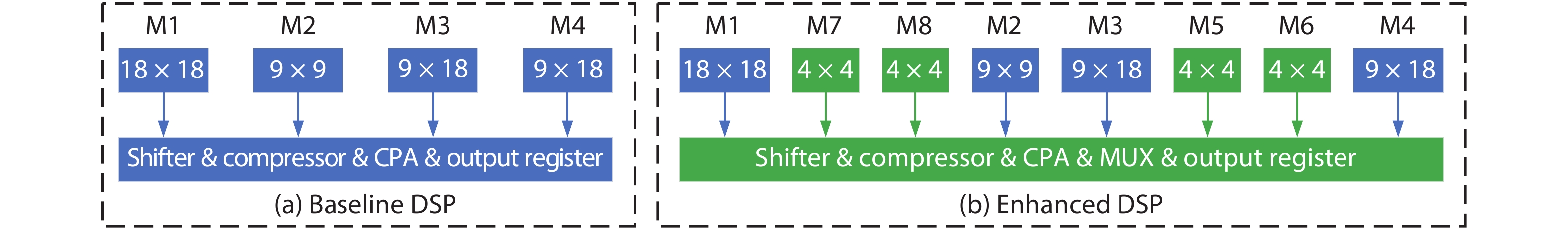
    First, they built a base-line DSP which looks like the one in Arria-10 Intel FPGA, it can perform one 27-bit multiplication, and two 18-bit multiplication. Its maximum operation frequency is 600 MHz. Fig. 1(a) shows the simplified architecture of base-line DSP.

    (Color online) Simplified architecture of (a) baseline DSP and (b) enhanced DSP.

    Figure 1.(Color online) Simplified architecture of (a) baseline DSP and (b) enhanced DSP.

    For one 27-bit multiplication, A[26:0] × B[26:0], A[26:9] × B[26:9] is implemented on 18 × 18 M1 multiplier, A[8:0] × B[8:0] is implemented on 9 × 9 M2 multiplier, A[8:0] × B[26:9] is implemented on 9 × 18 M3 multiplier, A[26:9] × B[8:0] is implemented on 9 × 18 M4 multiplier. For two 18-bit multiplication, one is implemented on 18 × 18 M1 multiplier, the other one is implemented on 9 × 18 M3 multiplier and 9 × 18 M4 multiplier. The 9 × 9 M2 multiplier is left unused.

    The enhanced DSP keeps working at 600 MHz frequency, without increasing the inputs and outputs, and ensure backward compatible to base-line DSP.

    The enhanced DSP support four 9-bit multiplication, because the baseline DSP has 72 (= 18 × 4) outputs. The four 9-bit multiplication is implemented on M1, M2, M3 and M4, with additional Shifter, Compressor and MUX.

    Boutros et al.[14] compare three different methods to implement eight 4-bit multiplication. The first one is to fracture each of M1, M2, M3 and M4, make each one perform 4-bit multiplication. The second one is to fracture M2 and M3 which is not on the critical path, and add four additional 4-bit multipliers. The last one is to fracture M2 and M3, make M1 and M4 to support one 4-bit multiplier each and add two additional 4-bit multipliers. From the experiment, the second solution is the best. Fig. 1(b) shows the simplified architecture of enhanced DSP block.

    From experiments, the enhanced DSP blocks can pack twice as many 9-bit and four times as many 4-bit multiplications as DSP blocks in Arria 10. Boutros et al.[14] use COFFE 2[23, 24] to evaluate enhanced DSP block’s area, the results show it has 12% more area than base-line DSP.

    Finally, Boutros et al. [14] evaluate performance of the enhanced DSP when implementing different CNN models at both 8-bit and 4-bit precision. They find FPGA with enhanced DSP uses less logic resources and achieves 1.62 × and 2.97 × higher performance respectively if just DSP is used to implement multiplication.

    DSP block of Intel AgileX can work at fixed-point four 9 × 9 multiplier adder mode[15], which supports for lower precision INT8 through INT2. This feature facilitates lower-precision, higher-performance inference. Xilinx ACAP also support INT8 computation, VC1902 of AI Core Series provides INT8 peak performance up to 13.6 TOP/s [25].

    2.2. Floating-point design

    Intel Arria 10[21] and Stratix 10[22] FPGA provides the industry first floating-point DSP. Intel AgileX FPGAs support Variable-precision DSP, it retains its leading floating-point performance, Intel added additional DSP hardware to achieve 40 TFLOPS of FP16 performance and added hardened Bfloat16 support[15]. The Bfloat16 (Brain Floating Point) floating-point format is a truncated (16-bit) version of the 32-bit single-precision floating-point format (binary32). It is used to accelerate machine learning.

    Previous DSP[26] of Xilinx FPGA does not support floating-point operation. The DSP Engine of ACAP[19] contains a floating-point multiplier and a floating-point adder. Each floating-point multiplier input can be in either binary32 (single-precision or FP32) or binary16 (half-precision or FP16) format. VC1902 of AI Core Series provides FP32 peak performance up to 3.2 TFLOP/s[25].

    3. ALM/CLB module design for AI

    As mentioned before, with acceptable accuracy, low-precision can improve FPGA MAC performance. Most MAC operation is done by DSP module in FPGA. But DSP blocks represent only 5% of the FPGA core area in DSP-rich devices[27]. Just enhancing the DSP block is not enough. ALM are the most abundant logic resource in Intel FPGA. ALM enhancements will impact more on MAC performance than DSP block enhancements.

    BNN[12] is an ultra-reduced precision version of DNN, at the same time, BNN can keep accuracy acceptable. BNN decreases memory and computation resources dramatically, and increase the computation performance. In order to increase the logic density of FPGA BNN implementations, ALM and CLB can be enhanced.

    3.1. Low-precision design

    Boutros et al.[16] make three different architectural enhancements to the ALM of Intel FPGAs to improve the density of on-chip low-precision MAC operations with minimal area and delay cost.

    Fig. 2(a) shows the first architecture enhancement, that is ALM with the proposed extra carry chain architecture modifications. Fig. 2(b) shows the second architecture enhancement, that is ALM with the proposed 4-bit adder architecture which fracture each 4-LUT into two 3-LUT and has two additional full adders and multiplexing. In this way, ALM can implement more adders. Fig. 2(c) shows the third architecture enhancement, that is LAB with the proposed shadow multiplier. When shallow multiplier works, the middle two ALMs is not available. In this way, it can increase the density of on-chip MAC operation.

    (Color online) Proposed extra carry chain architecture modifications.

    Figure 2.(Color online) Proposed extra carry chain architecture modifications.

    Boutros et al.[16] extended the COFFE 2[23, 24] to support these three architectures, and used it to generate detailed area and delay values. With minimal area and delay cost, the extra carry chain architecture can achieve a 21% and a 35% reduction in average MAC delays and areas, respectively. The 4-bit Adder architecture achieves similar results compared to extra carry chain architecture.

    Combining shadow multiplier and 4-bit adder architectures can get the best result which increase 6.1 × MAC density, it also leads to larger tile area and larger critical path delay value.

    3.2. BNN design

    For each layer of neural network of BNN, the input (except for original input), the weights and activations are binarized (+1 or –1), which can be represented by 1-bit (see Fig. 3(b)). Figs. 3(a) and 3(b) make a comparison of flow between CNN and BNN.

    (Color online) The difference of CNN and BNN: (a) CNN, (b) BNN and (c) XNOR replace multiplication for BNN.

    Figure 3.(Color online) The difference of CNN and BNN: (a) CNN, (b) BNN and (c) XNOR replace multiplication for BNN.

    The convolutional operation of CNN is multiply-accumulation. For BNN, we can use 1 to represent +1, use 0 to represent –1, so the multiplication can transform to XNOR operation. See Fig. 3(c). Then the accumulation operation can transform to popcount operation which is to count the number of ones in a large word. Thus, the MAC operation of a BNN is reduced to XNOR-popcount operation which can easily implemented on FPGA. And the weights and activations of BNN is 1-bit, makes it possible to store all parameters on chip memory of FPGA.

    On an FPGA, the XNOR part is easily implemented with LUTs. For the popcount part, it is common to use a binary full adder tree to sum up the bits in vectors. This requires N − 1 binary adders in different bit-width[2]. For long vectors, this process requires more LUT resources.

    Kim et al.[18] propose two ALM modifications that improve the logic density of FPGA BNN implementations. For the first ALM modification, Kim et al.[18] propose additional carry-chain circuitry in an ALM. Instead of propagating carry, it propagates sum. The sum-out can propagate to the carry-in of the next adder. In this way, it creates a chain of sum.

    This ALM modification only adds two dedicated ports in carry-chain direction, it doesn’t add other ports to ALM, so it does not affect the general routing circuit. This ALM modification allows two carry-chains to be used in two distinct modes. For the first mode, it uses the original carry chain, and outputs the sum result. For the second mode, it uses a new carry chain to perform popcount operation, and outputs carry result. Fig. 4(a) shows the first ALM modification for BNN, that is ALM with the proposed extra charry chain which propagates sum.

    (Color online) ALM modifications: (a) ALM modification 1 and (b) ALM modification 2.

    Figure 4.(Color online) ALM modifications: (a) ALM modification 1 and (b) ALM modification 2.

    For the second ALM modification, Kim et al.[18] propose to add an additional FA (full adder) on top of ALM modification 1 (see Fig. 4(b)). The ALM modification 1 build the first level of the popcount adder tree within an ALM. The ALM modification 2 with one additional FA wants to build the second level of popcount adder tree. In this way, two levels of popcount adder tree are incorporated in one ALM. So, the total ALM modifications include one carry chain (two adders) which propagates sum-out, and one FA.

    Two architecture changes need to add corresponding SRAM to configurate MUX select port. Kim et al.[18] also make the similar architecture changes to the Xilinx FPGA. Through the experiments, the first change reduces ALM/LUT usage by 23%–44%, across a range of XNOR-popcount widths, depending on the vendor. The second change reduces ALM/LUT usage by 39%–60%[18].

    4. Memory module design for AI

    Xilinx ACAP[16] provides more memory resources which includes distributed-RAM, 36 Kb block RAM and 288 Kb UltraRAM. The upcoming Versal HBM series which aims for data left market, are premium platform with HBM. ACAP also provide memory interfaces such as DDR4/LPDDR4. Some Versal ACAPs include Accelerator RAM, an additional 4 MB of on-chip memory[19].

    Intel Agilex[15] FPGAs provide a broad hierarchy of memory resources, including embedded memory resources, in package memory, and off-chip memory via dedicated interfaces (see Fig. 5(b)). Embedded memory includes 640-bit MLABs, 20 kB block RAM, and 18.432 MB eSRAM. In package memory is HBM, which reduces board size, cost and power requirements. Off-chip memory are interfaces to memory components external to the device, including advanced memory types like DDR5 and Intel Optane DC persistent memory. Other interfaces are DDR4, QDR, and RLDRAM.

    (Color online) Intel AgileX Architecture. (a) AgileX Architecture. (b) Advanced memory hierarchy.

    Figure 5.(Color online) Intel AgileX Architecture. (a) AgileX Architecture. (b) Advanced memory hierarchy.

    5. Other designs for AI

    5.1. Acceleration platform

    At June 18th 2019, Xilinx announced that it has shipped VersalTM AI Core series and Versal Prime series devices. Versal devices are industry first adaptive compute acceleration platform (ACAP) which uses TSMC's 7 nm manufacturing process technology. ACAP[16] includes scalar engines, adaptable engines, intelligent engines, HBM, PCIe, etc. The NoC connects them all together, and provides high-bandwidth. See Fig. 6(a).

    (Color online) ACAP Architecture. (a) ACAP architecture. (b) AI engine.

    Figure 6.(Color online) ACAP Architecture. (a) ACAP architecture. (b) AI engine.

    The scalar engines include the dual-core Arm® Cortex-A72 and dual-core Arm® Cortex-R5. The adaptable engines are previous FPGA fabric, it is comprised of programmable logic and memory cells. The intelligence engines contain AI engines and DSP engines. ACAP achieves dramatic performance improvements of up to 20 × over today's fastest FPGA implementations and over 100 × over today's fastest CPU implementations—for Data Center, 5G wireless and AI, etc.[16].

    5.2. Compute-intensive processor

    Xilinx design the specialized AI engine[16, 19, 20] to meet the demand of compute-intensive DNN application, AI engines[16, 20] can provide up to 8X silicon compute density at 50% the power consumption compared to traditional programmable logic solutions. The AI engine contains: a high-performance VLIW vector (SIMD) processor which is 1 GHz+ multi-precision vector processor; integrated data memory which can be extended to high bandwidth memory; and interconnects for streaming, configuration, and debug. See Fig. 6(b).

    For a CNN model, AI engines can perform convolution layers, fully connected layers, and activation function (Relu, Sigmoid, etc.). While programmable logic can implement pooling function (Max Pool), and store weights and activation values in UltraRAM.

    5.3. FPGA-CPU platform

    On August 29th 2019, Intel has begun shipments of the first 10 nm Agilex FPGAs. Agilex aims to deal with the data proliferation problem the edge to the network to the cloud, it is a data-centric product.

    What it is most important is that AgileX supports compute express link, which enables a high-speed and memory coherent interconnect to future Intel Xeon scalable processors. Other innovations include: 2nd generation HyperFlex, embedded multi-die interconnect bridge (EMIB), PCIe Gen 5, variable-precision DSP, advanced memory hierarchy, Quad-core A53 HPS, 112 Gbps transceiver, etc. See Fig. 5(a). AgileX delivers up to 40% higher core performance, or up to 40% lower power over previous generation high-performance FPGAs[28].

    6. Conclusion

    Reconfigurability, low-power and real-time makes FPGA excel at inference tasks. The FPGA chip has to redesign to better implement different evolving DNN requirements. Table 1 shows the summary of all enhancements of FPGA for the AI era.

    Table Infomation Is Not Enable

    For the DSP module, in order to support low-precision techniques, Boutros et al. enhance DSP block to support 9-bit and 4-bit multiplication. DSP of Intel AgileX supports INT8 computation. In order to support high-accuracy, Intel and Xilinx design their DSP to support float point computation. For ALM module, Boutros et al. enhance ALM with extra carry chain, or more adders, or shadow multipliers modification increase the density of on-chip MAC operation. Kim et al. propose two modifications on ALM and CLB (configurable logic block) better support BNN implementation. For memory module, ACAP of Xilinx and Agilex of Intel provide more memory resources which include three types of memory which are embedded memory, in-package HBM (high bandwidth memory) and off-chip memory interfaces, such as DDR4/5.

    Other design considerations include new architecture or specialized AI processor. Xilinx ACAP in 7 nm is the first industry adaptive compute acceleration platform. ACAP also provides specialized AI engine which can increase compute density by 8X with 50% lower power. Intel AgileX in 10 nm works coherently with Intel own CPU, which increase performance, reduced overhead and latency.

    References

    [1] A Krizhevsky, I Sutskever, G E Hinton. ImageNet classification with deep convolutional neural networks. Neural Information Processing Systems (NIPS), 1097(2012).

    [2] S Liang, S Yin, L Liu et al. FP-BNN: Binarized neural network on FPGA. Neurocomputing, 275, 1072(2017).

    [3]

    [4] C Zhang, P Li, G Sun et al. Optimizing FPGA-based accelerator design for deep convolutional neural networks. The 2015 ACM/SIGDA International Symposium on Field-Programmable Gate Arrays, 161(2015).

    [5] J Qiu, J Wang, S Yao et al. Going deeper with embedded FPGA platform for convolutional neural network. The 2016 ACM/SIGDA International Symposium on Field-Programmable Gate Arrays, 26(2016).

    [6] S Yin, P Ouyang, S Tang et al. A high energy efficient reconfigurable hybrid neural network processor for deep learning applications. IEEE J Solid-State Circuits, 53, 968(2018).

    [7] S Han, H Mao, W J Dally. Deep compression: compressing deep neural networks with pruning, trained quantization and huffman coding. ICLR(2016).

    [8] P Gysel, M Motamedi, S Ghiasi. Hardware-oriented approximation of convolutional neural networks. ICLR(2016).

    [9] S Han, X Liu, H Mao et al. EIE: efficient inference engine on compressed deep neural network. International Symposium on Computer Architecture (ISCA), 243(2016).

    [10] A Zhou, A Yao, Y Guo et al. Incremental network quantization: towards lossless CNNs with low-precision weights. ICLR(2017).

    [11]

    [12] I Hubara, M Courbariaux, D Soudry. Binarized neural networks. Neural Information Processing Systems (NIPS), 1(2016).

    [13] Y Umuroglu, N J Fraser, G Gambardella et al. FINN: A framework for fast, scalable binarized neural network inference. International Symposium on Field-Programmable Gate Arrays, 65(2017).

    [14] A Boutros, S Yazdanshenas, V Betz. Embracing diversity: Enhanced DSP blocks for low precision deep learning on FPGAs. 28th International Conference on Field-Programmable Logic and Applications, 35(2018).

    [15]

    [16]

    [17] A Boutros, M Eldafrawy, S Yazdanshenas et al. Math doesn’t have to be hard: logic block architectures to enhance low-precision multiply-accumulate on FPGAs. The 2019 ACM/SIGDA International Symposium on Field-Programmable Gate Arrays, 94(2019).

    [18] J H Kim, J Lee, J H Anderson. FPGA architecture enhancements for efficient BNN implementation. International Conference on Field-Programmable Technology (ICFPT), 217(2018).

    [19]

    [20]

    [21]

    [22]

    [23] S Yazdanshenas, V Betz. Automatic circuit design and modelling for heterogeneous FPGAs. International Conference on Field-Programmable Technology (ICFPT), 9(2017).

    [24] S Yazdanshenas, V Betz. COFFE 2: Automatic modelling and optimization of complex and heterogeneous FPGA architectures. ACM Trans Reconfig Technol Syst, 12, 3(2018).

    [25]

    [26]

    [27] M Langhammer, B Pasca. Floating-point DSP block architecture for FPGAs. The 2015 ACM/SIGDA International Symposium on Field-Programmable Gate Arrays, 117(2015).

    [28]

    Zhengjie Li, Yufan Zhang, Jian Wang, Jinmei Lai. A survey of FPGA design for AI era[J]. Journal of Semiconductors, 2020, 41(2): 021402
    Download Citation