• Advanced Photonics
  • Vol. 2, Issue 5, 054002 (2020)
Mark I. Stockman*
Author Affiliations
  • Georgia State University, Center for Nano-Optics (CeNO), Department of Physics and Astronomy, Atlanta, Georgia, United States
  • show less
    DOI: 10.1117/1.AP.2.5.054002 Cite this Article Set citation alerts
    Mark I. Stockman. Brief history of spaser from conception to the future[J]. Advanced Photonics, 2020, 2(5): 054002 Copy Citation Text show less
    Conceptual schematic of a realistic nanospaser geometry, composition, and its action principle. (a) Schematic of geometry and composition of a nanoshell spaser with gain medium outside. The local fields (per one plasmon in a dipolar spasing mode) are shown by color coding by the bar to the right. Plasmonic nanoshell and gain medium (orange dots) are indicated. (b) The same as (a) but for the gain medium inside the shell. (c) Schematic of the spaser functioning. Energy levels of the gain medium are depicted to the left and of the plasmonic core (the nanoshell in this case) are shown to the right. External source (optical or electrical, indicated by a vertical black arrow) injects electrons into the CB creating nonequilibrium (hot) electron–hole plasma. The hot carriers relax to the bandgap (vertical green arrow), possibly forming excitons. These excitations decay without radiation by transferring their energy to LSPs of the nanoshell (shown by coupled red arrows). These SPs stimulate emission of more SPs causing an avalanche of generation eventually stabilized by the saturation of the gain medium. Adapted from Refs. 4 and 57.
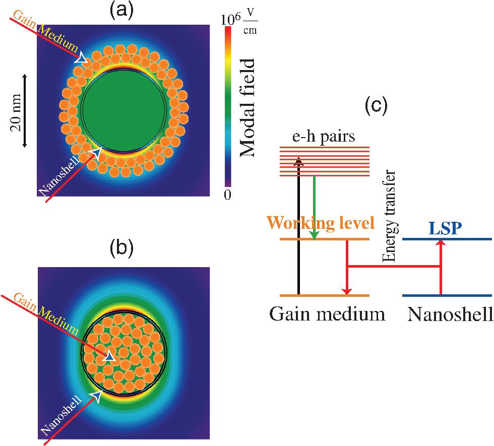
    Fig. 1. Conceptual schematic of a realistic nanospaser geometry, composition, and its action principle. (a) Schematic of geometry and composition of a nanoshell spaser with gain medium outside. The local fields (per one plasmon in a dipolar spasing mode) are shown by color coding by the bar to the right. Plasmonic nanoshell and gain medium (orange dots) are indicated. (b) The same as (a) but for the gain medium inside the shell. (c) Schematic of the spaser functioning. Energy levels of the gain medium are depicted to the left and of the plasmonic core (the nanoshell in this case) are shown to the right. External source (optical or electrical, indicated by a vertical black arrow) injects electrons into the CB creating nonequilibrium (hot) electron–hole plasma. The hot carriers relax to the bandgap (vertical green arrow), possibly forming excitons. These excitations decay without radiation by transferring their energy to LSPs of the nanoshell (shown by coupled red arrows). These SPs stimulate emission of more SPs causing an avalanche of generation eventually stabilized by the saturation of the gain medium. Adapted from Refs. 4 and 57.
    All-color InGaN@GaN nanorod spasers (plasmonic nanolasers). (a) Schematic diagram of the nanospaser structure: single InxGa1−xN@GaN core–shell nanorods were dispersed on the Al2O3-covered epitaxial Ag film. The scanning electron microscopy (SEM) image on the upper right indicates that one can measure the laser emissions from individual single nanorods with a collection area of about 3 μm in diameter using a focused excitation laser beam. (b) All-color, single-mode lasing images observed from single nanorods with an emission line width ∼4 nm. (c) The simulated energy density distribution of a blue (474 nm) nanospaser. The resonant field is tightly confined in the 5 nm, low-index (n≈1.77) Al2O3 gap layer grown by ALD, and the plasmonic cavity mode is formed between the nanorod and the epitaxial Ag film. (d) Concurrent RGB lasing from three nanorods placed close to each other. The optical pumping source is a 405-nm, CW semiconductor laser diode with an excitation power density of 3.9 kW/cm2. The scale bar represents 5 μm. (e) An ultrasmall plasmonic nanolaser (spaser) emitting at 627 nm (red) that is pumped below (0.4 Ith) and above (2.4 Ith) the spasing threshold. Both the OM images and the emission spectra show that a strong frequency pulling effect occurs during transition from spontaneous emission (642 nm) to lasing (627 nm). Adapted from Ref. 29.
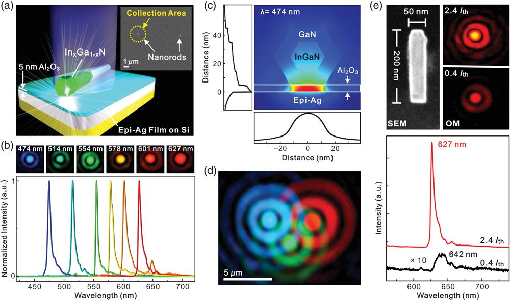
    Fig. 2. All-color InGaN@GaN nanorod spasers (plasmonic nanolasers). (a) Schematic diagram of the nanospaser structure: single InxGa1xN@GaN core–shell nanorods were dispersed on the Al2O3-covered epitaxial Ag film. The scanning electron microscopy (SEM) image on the upper right indicates that one can measure the laser emissions from individual single nanorods with a collection area of about 3  μm in diameter using a focused excitation laser beam. (b) All-color, single-mode lasing images observed from single nanorods with an emission line width 4  nm. (c) The simulated energy density distribution of a blue (474 nm) nanospaser. The resonant field is tightly confined in the 5 nm, low-index (n1.77) Al2O3 gap layer grown by ALD, and the plasmonic cavity mode is formed between the nanorod and the epitaxial Ag film. (d) Concurrent RGB lasing from three nanorods placed close to each other. The optical pumping source is a 405-nm, CW semiconductor laser diode with an excitation power density of 3.9  kW/cm2. The scale bar represents 5  μm. (e) An ultrasmall plasmonic nanolaser (spaser) emitting at 627 nm (red) that is pumped below (0.4Ith) and above (2.4Ith) the spasing threshold. Both the OM images and the emission spectra show that a strong frequency pulling effect occurs during transition from spontaneous emission (642 nm) to lasing (627 nm). Adapted from Ref. 29.
    Spectral and temperature dependence of spasing threshold and line width. (a) Characteristic L–L plots measured from individual RGB nanolasers. The pumping laser polarization direction was chosen to be perpendicular to the rod axis. Here, plots of the emission peak intensity versus the CW pumping intensity (L–L plots) for blue (474 nm), green (554 nm), and red (627 nm) spasers (plasmonic nanolasers) are shown for comparison. The different onsets of kinks in the L–L plots indicate that the lasing thresholds are 140 and 100 W/cm2, and undetectably small (<10 W/cm2) for red, green, and blue nanolasers, respectively. The fitted spontaneous emission coupling factors (β) of RGB nanolasers are found to be ∼0.3 (red), ∼0.7 (green), and ∼1.0 (blue) using a rate equation model. (b) Temperature-dependent L–L plots showing lasing thresholds at temperatures varied from 7 to 120 K for the blue (474 nm) nanolaser shown in (a), which exhibits an undetectable lasing threshold at 7 K. The inset shows the measured temperature dependence of the lasing threshold. (c) Temperature evolution of the spectral line width for two blue-emitting nanorods measured with and without the plasmonic cavity at varied temperatures from 7 to 300 K. These measurements were performed at a fixed pump intensity of 30 W/cm2, as shown in (b). The cyan dots represent measurement results for a single InGaN @GaN core–shell nanorod placed directly on a silicon substrate and emitting at 475 nm (RT). The fitted curve exhibits a typical PL line width narrowing behavior. In contrast, the blue dots show the measurement results for the blue (474 nm) nanolaser case with the plasmonic core (cavity), where we discover a characteristic staircase line width narrowing behavior. Three line width regions can be identified that include the lasing region (I; ∼4 nm for T<40 K), the SP-coupled PL region (II; ∼8 nm for temperature 40 K<T<100 K), and the gain-medium PL region (III; 100 K<T<300 K), respectively. (d) To confirm the lasing behavior in the time domain, second-order photon correlation functions were measured under the same pump intensity (270 W/cm2) at 80 and 7 K, respectively. As shown in (b), the pump intensity is right below the lasing threshold at 80 K. Indeed, g(2)(0) is measured to be greater than one, as expected for the case of thermal emission. In comparison, when the pump intensity is above the lasing threshold at 7 K, we confirm that g(2)(0)=1 and remains at unity for all τ, which is an unambiguous signature of nanolasing (spasing), which is due to a rapid recovery of plasmon population after the emission of a quantum. Adapted from Ref. 29.
    Fig. 3. Spectral and temperature dependence of spasing threshold and line width. (a) Characteristic L–L plots measured from individual RGB nanolasers. The pumping laser polarization direction was chosen to be perpendicular to the rod axis. Here, plots of the emission peak intensity versus the CW pumping intensity (L–L plots) for blue (474 nm), green (554 nm), and red (627 nm) spasers (plasmonic nanolasers) are shown for comparison. The different onsets of kinks in the L–L plots indicate that the lasing thresholds are 140 and 100  W/cm2, and undetectably small (<10  W/cm2) for red, green, and blue nanolasers, respectively. The fitted spontaneous emission coupling factors (β) of RGB nanolasers are found to be 0.3 (red), 0.7 (green), and 1.0 (blue) using a rate equation model. (b) Temperature-dependent L–L plots showing lasing thresholds at temperatures varied from 7 to 120 K for the blue (474 nm) nanolaser shown in (a), which exhibits an undetectable lasing threshold at 7 K. The inset shows the measured temperature dependence of the lasing threshold. (c) Temperature evolution of the spectral line width for two blue-emitting nanorods measured with and without the plasmonic cavity at varied temperatures from 7 to 300 K. These measurements were performed at a fixed pump intensity of 30  W/cm2, as shown in (b). The cyan dots represent measurement results for a single InGaN @GaN core–shell nanorod placed directly on a silicon substrate and emitting at 475 nm (RT). The fitted curve exhibits a typical PL line width narrowing behavior. In contrast, the blue dots show the measurement results for the blue (474 nm) nanolaser case with the plasmonic core (cavity), where we discover a characteristic staircase line width narrowing behavior. Three line width regions can be identified that include the lasing region (I; 4  nm for T<40  K), the SP-coupled PL region (II; 8  nm for temperature 40  K<T<100  K), and the gain-medium PL region (III; 100  K<T<300  K), respectively. (d) To confirm the lasing behavior in the time domain, second-order photon correlation functions were measured under the same pump intensity (270  W/cm2) at 80 and 7 K, respectively. As shown in (b), the pump intensity is right below the lasing threshold at 80 K. Indeed, g(2)(0) is measured to be greater than one, as expected for the case of thermal emission. In comparison, when the pump intensity is above the lasing threshold at 7 K, we confirm that g(2)(0)=1 and remains at unity for all τ, which is an unambiguous signature of nanolasing (spasing), which is due to a rapid recovery of plasmon population after the emission of a quantum. Adapted from Ref. 29.
    (a) Sensing is based on the intensity change in stimulated emission from an SPP nanolaser with subwavelength electromagnetic field confinement, where the semiconductor slab provides optical gain as well as acts as a sensing material. (b) SEM image of the device, which consists of a CdS nanoslab (thickness, d1, 50 nm; length, 600 nm) on top of an Ag film, separated by an 8-nm d2 low-permittivity MgF2 layer. (c) Measured spectra of the emission from the SPP nanolaser under N2 and 8 ppb 2,4-dinitrotoluene (DNT). (d) Red diamonds: continuous trace of emission intensities of the active plasmon nanosensor when delivering DNT vapor at concentrations of 1, 2, 4, and 8 ppb. Black line: guide to the eye. Green circles: the tracked lasing peak wavelength obtained by Gaussian fitting of the spectra. There is no appreciable change in the peak wavelength at various DNT concentrations, which indicates that directly monitoring the lasing intensity has superior performance than monitoring the index-change-induced peak wavelength shift in active plasmon sensors. Adapted from Ref. 30.
    Fig. 4. (a) Sensing is based on the intensity change in stimulated emission from an SPP nanolaser with subwavelength electromagnetic field confinement, where the semiconductor slab provides optical gain as well as acts as a sensing material. (b) SEM image of the device, which consists of a CdS nanoslab (thickness, d1, 50 nm; length, 600 nm) on top of an Ag film, separated by an 8-nm d2 low-permittivity MgF2 layer. (c) Measured spectra of the emission from the SPP nanolaser under N2 and 8 ppb 2,4-dinitrotoluene (DNT). (d) Red diamonds: continuous trace of emission intensities of the active plasmon nanosensor when delivering DNT vapor at concentrations of 1, 2, 4, and 8 ppb. Black line: guide to the eye. Green circles: the tracked lasing peak wavelength obtained by Gaussian fitting of the spectra. There is no appreciable change in the peak wavelength at various DNT concentrations, which indicates that directly monitoring the lasing intensity has superior performance than monitoring the index-change-induced peak wavelength shift in active plasmon sensors. Adapted from Ref. 30.
    Sensing with a nanoslab SPP spaser. (a) Device schematics in side view. A nanoslab of the gain medium crystal is deposited upon a nanofilm of MgF2 covering a surface of gold. The device is protected by a nanometric film of Al2O3 insulator. (b) A SEM image of the fabricated device consisting of a CdSe nanoslab atop of Au substrate separated by a few nanometers MgF2. The band edge emission of CdSe is around 700 nm located in the preferred sensing region. The Au is chosen because it is much more stable compared to silver. The scale bar is 2 μm. (c) Emission spectra with the working mode at ∼718 nm. The overlapped spectra indicate no observable lasing intensity decrease with the operation duration. (d) Full emission spectra of the device in the five solutions with varied refractive indexes. A red frequency shift is manifest when the ambient index increases by just ∼10−3. Adapted from Refs. 43 and 44.
    Fig. 5. Sensing with a nanoslab SPP spaser. (a) Device schematics in side view. A nanoslab of the gain medium crystal is deposited upon a nanofilm of MgF2 covering a surface of gold. The device is protected by a nanometric film of Al2O3 insulator. (b) A SEM image of the fabricated device consisting of a CdSe nanoslab atop of Au substrate separated by a few nanometers MgF2. The band edge emission of CdSe is around 700 nm located in the preferred sensing region. The Au is chosen because it is much more stable compared to silver. The scale bar is 2  μm. (c) Emission spectra with the working mode at 718  nm. The overlapped spectra indicate no observable lasing intensity decrease with the operation duration. (d) Full emission spectra of the device in the five solutions with varied refractive indexes. A red frequency shift is manifest when the ambient index increases by just 103. Adapted from Refs. 43 and 44.
    Structure and spectra of spasers. (a) Schematic of nanoshell spaser (left) and its functioning inside a living cell. The spaser consists of a gold nanosphere core surrounded by a porous silica shell impregnated with a dye (uranine). Schematic of a cell (right) and processes accompanying pulsed spasing. A pump laser pulse causes spaser generation where stimulated optical emission occurs, a vapor bubble is formed due to the heat production and shock wave, and acoustic waves are launched. (b) Spectra of spasers investigated: nanoshell with uranine dye, nanoshell with fluorescein dye, and three gold nanorods surrounded by shells with the DCM dye. For comparison, the spectrum of QD radiation is shown magnified 25×. Electron micrographs of a 20-nm spherical spaser and a 50-nm nanorod spaser are shown at the top. (c) Red line: radiation intensity of spaser as a function of the pump fluence (L–P line). Blue line: linewidth of the spaser radiation as a function of the pump fluence. Insets: optical micrograph of the operating spaser. Adapted from Ref. 40.
    Fig. 6. Structure and spectra of spasers. (a) Schematic of nanoshell spaser (left) and its functioning inside a living cell. The spaser consists of a gold nanosphere core surrounded by a porous silica shell impregnated with a dye (uranine). Schematic of a cell (right) and processes accompanying pulsed spasing. A pump laser pulse causes spaser generation where stimulated optical emission occurs, a vapor bubble is formed due to the heat production and shock wave, and acoustic waves are launched. (b) Spectra of spasers investigated: nanoshell with uranine dye, nanoshell with fluorescein dye, and three gold nanorods surrounded by shells with the DCM dye. For comparison, the spectrum of QD radiation is shown magnified 25×. Electron micrographs of a 20-nm spherical spaser and a 50-nm nanorod spaser are shown at the top. (c) Red line: radiation intensity of spaser as a function of the pump fluence (L–P line). Blue line: linewidth of the spaser radiation as a function of the pump fluence. Insets: optical micrograph of the operating spaser. Adapted from Ref. 40.
    Spasers inside a cancer cell. (a) Optical micrograph of a single spaser radiating inside a cell. (b) Optical micrograph of multiple spasers generated inside cancer cells. (c) Electron micrograph (positive contrast) of multiple spasers inside a cell. Single spaser, dimer of the spasers, and cluster of multiple spasers are clearly seen. (d) Photothermal image of a cell labeled with multiple spasers. (e) Optical micrograph showing a single spaser (marked by a white arrow) producing a vapor bubble around it. (f) Optical micrograph illustrating mechanism of cancer therapeutics using spasers. A single spaser surrounded by a vapor bubble is indicated by a white arrow. Red arrows indicate fragments of the cell membrane damage due to shock waves produced by the cavitation around the spaser. The cancer cell dyes after one or a few laser pulses. Adapted from Ref. 40.
    Fig. 7. Spasers inside a cancer cell. (a) Optical micrograph of a single spaser radiating inside a cell. (b) Optical micrograph of multiple spasers generated inside cancer cells. (c) Electron micrograph (positive contrast) of multiple spasers inside a cell. Single spaser, dimer of the spasers, and cluster of multiple spasers are clearly seen. (d) Photothermal image of a cell labeled with multiple spasers. (e) Optical micrograph showing a single spaser (marked by a white arrow) producing a vapor bubble around it. (f) Optical micrograph illustrating mechanism of cancer therapeutics using spasers. A single spaser surrounded by a vapor bubble is indicated by a white arrow. Red arrows indicate fragments of the cell membrane damage due to shock waves produced by the cavitation around the spaser. The cancer cell dyes after one or a few laser pulses. Adapted from Ref. 40.
    Use of spasers for STED super-resolution imaging. (a) Emission spectrum of the gain-medium dye (a fluorescein derivative) (red dashed line) and the spasing spectral line (solid black peak). An electron micrograph of the spasers is shown in the inset. (b) Optical image of generating spaser aggregates in a confocal microscope. (c) The same as in (b) but using STED super-resolution microscopy. (d) Confocal optical image of separated single spasers. (e) The same as in (d) but using STED super-resolution microscopy. Adapted from Ref. 58.
    Fig. 8. Use of spasers for STED super-resolution imaging. (a) Emission spectrum of the gain-medium dye (a fluorescein derivative) (red dashed line) and the spasing spectral line (solid black peak). An electron micrograph of the spasers is shown in the inset. (b) Optical image of generating spaser aggregates in a confocal microscope. (c) The same as in (b) but using STED super-resolution microscopy. (d) Confocal optical image of separated single spasers. (e) The same as in (d) but using STED super-resolution microscopy. Adapted from Ref. 58.
    Concept of ∼300 MHz C-MOS processor with a low energy cost per flop. (a) Schematic of existing C-MOS technology. A pair of complementary MOS transistors is connected with a copper nanowire interconnect (right and left panels). Middle panel shows a cross section of a processor chip where interconnects dominate the entire volume and consume 99% of the energy. (b) A concept of the spaser-powered interconnect processing. The same pair of C-MOS transistors is not connected electrically. Instead, a controlling NMOS transistor directly powers a spaser that sends an SPP pulse along a copper interconnect wire without charging it. The SPP pulse is transformed back to an electrical pulse by a Ge phototransistor and then fed to the gate of the receiving PMOS transistor. Adapted from Ref. 47.
    Fig. 9. Concept of 300  MHz C-MOS processor with a low energy cost per flop. (a) Schematic of existing C-MOS technology. A pair of complementary MOS transistors is connected with a copper nanowire interconnect (right and left panels). Middle panel shows a cross section of a processor chip where interconnects dominate the entire volume and consume 99% of the energy. (b) A concept of the spaser-powered interconnect processing. The same pair of C-MOS transistors is not connected electrically. Instead, a controlling NMOS transistor directly powers a spaser that sends an SPP pulse along a copper interconnect wire without charging it. The SPP pulse is transformed back to an electrical pulse by a Ge phototransistor and then fed to the gate of the receiving PMOS transistor. Adapted from Ref. 47.
    Mark I. Stockman. Brief history of spaser from conception to the future[J]. Advanced Photonics, 2020, 2(5): 054002
    Download Citation