• Journal of Infrared and Millimeter Waves
  • Vol. 40, Issue 2, 172 (2021)
Da-Nong ZHENG1、2, Xiang-Bin SU1、2、*, Ying-Qiang XU1、2, and Zhi-Chuan NIU1、2
Author Affiliations
  • 1State Key Laboratory for Superlattices and Microstructures,Institute of Semiconductors,Chinese Academy of Sciences,Beijing 100083,China
  • 2College of Materials Science and Opto-Electronic Technology,University of Chinese Academy of Sciences,Beijing 101408,China
  • show less
    DOI: 10.11972/j.issn.1001-9014.2021.02.006 Cite this Article
    Da-Nong ZHENG, Xiang-Bin SU, Ying-Qiang XU, Zhi-Chuan NIU. High gain and low dark current AlInAsSb avalanche photodiodes grown by quaternary digital alloys[J]. Journal of Infrared and Millimeter Waves, 2021, 40(2): 172 Copy Citation Text show less
    Shutter sequences in a period of AlInAsSb digital alloy lattice-matched to GaSb for MEE growth method.
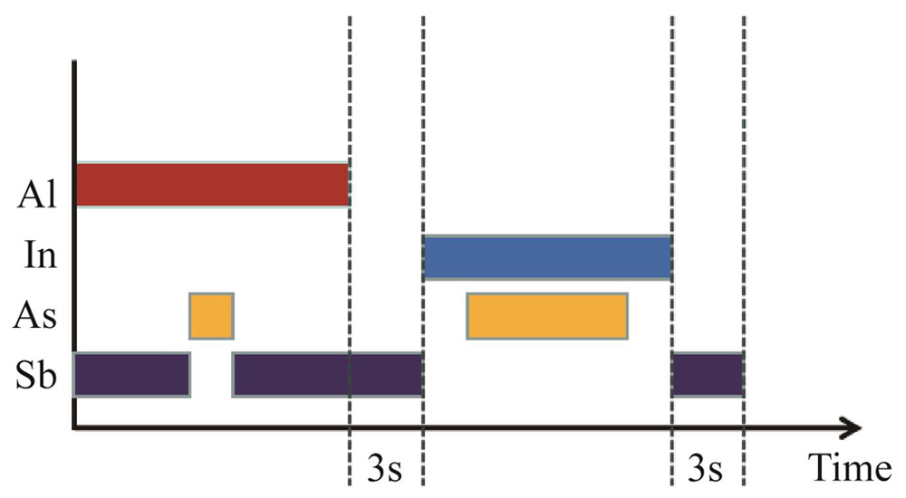
    Fig. 1. Shutter sequences in a period of AlInAsSb digital alloy lattice-matched to GaSb for MEE growth method.
    Schematic cross section of AlInAsSb DA SAGCM APD
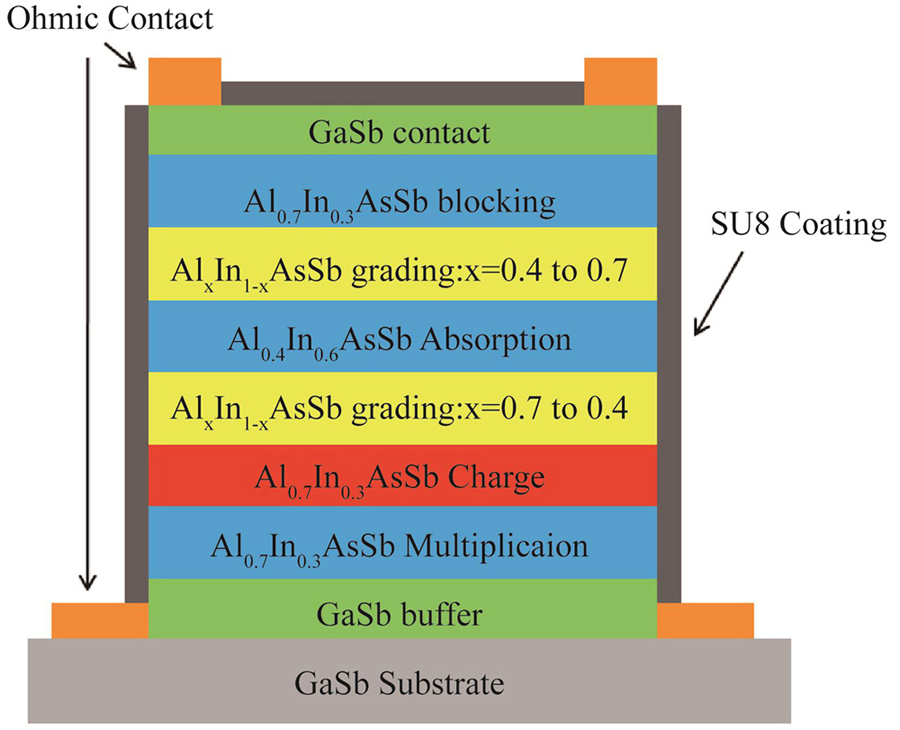
    Fig. 2. Schematic cross section of AlInAsSb DA SAGCM APD
    (a) HRXRD of Al0.7In0.3AsSb DA layer, (b) AFM of Al0.7In0.3AsSb DA layer
    Fig. 3. (a) HRXRD of Al0.7In0.3AsSb DA layer, (b) AFM of Al0.7In0.3AsSb DA layer
    (a) Epitaxial structure of AlxIn1-xAsSb DA grading layer, (b) HRXRD of AlxIn1-xAsSb DA grading layer, (c) AFM of AlxIn1-xAsSb DA grading layer
    Fig. 4. (a) Epitaxial structure of AlxIn1-xAsSb DA grading layer, (b) HRXRD of AlxIn1-xAsSb DA grading layer, (c) AFM of AlxIn1-xAsSb DA grading layer
    (a) HRXRD of Al0.4In0.6AsSb DA layer, (b) AFM of Al0.4In0.6AsSb DA layer
    Fig. 4. (a) HRXRD of Al0.4In0.6AsSb DA layer, (b) AFM of Al0.4In0.6AsSb DA layer
    (a) Dark current, photocurrent, multiplication factor versus reverse bias of a 200 μm-diameter AlInAsSb DA SAGCM APD at room temperature, (b) measured capacitance versus bias of a typical 200 μm-diameter AlInAsSb DA SAGCM APD at room temperature
    Fig. 6. (a) Dark current, photocurrent, multiplication factor versus reverse bias of a 200 μm-diameter AlInAsSb DA SAGCM APD at room temperature, (b) measured capacitance versus bias of a typical 200 μm-diameter AlInAsSb DA SAGCM APD at room temperature
    xAlSb/MLAlAs/MLAlSb/MLInSb/MLInAs/MLInSb/ML
    0.41.870.261.870.355.300.35
    0.52.290.432.280.354.300.35
    0.62.700.612.690.353.300.35
    0.73.090.823.090.352.300.35
    Table 1. Thickness of each layer in a period of AlxIn1-xAsySb1-ydigital alloy
    厚度/nm外延层材料

    掺杂浓度

    /cm-3

    50GaSb(Be)p contactp = 1.00×10¹⁹
    100Al0.7In0.3AsSb DA(Be)pp = 2×10¹⁸
    50AlxIn1-xAsSb DA grading:UID(非故意掺杂)
    1 000Al0.4In0.6AsSb DA absorptionUID
    50AlxIn1-xAsSb DA grading:UID
    100Al0.7In0.3AsSb DA(Be)chargep = 1.5×10¹⁷
    500Al0.7In0.3AsSb DA multiplicationUID
    500GaSb(Te)nn= 1 ×10¹⁸
    Table 2. Epitaxial structure of AlInAsSb DA SAGCM APD
    Da-Nong ZHENG, Xiang-Bin SU, Ying-Qiang XU, Zhi-Chuan NIU. High gain and low dark current AlInAsSb avalanche photodiodes grown by quaternary digital alloys[J]. Journal of Infrared and Millimeter Waves, 2021, 40(2): 172
    Download Citation