• Advanced Photonics
  • Vol. 6, Issue 3, 036001 (2024)
Hua Lu*, Shouhao Shi, Dikun Li, Shuwen Bo, Jianxu Zhao, Dong Mao, and Jianlin Zhao*
Author Affiliations
  • Northwestern Polytechnical University, School of Physical Science and Technology, MOE Key Laboratory of Material Physics and Chemistry under Extraordinary Conditions, Key Laboratory of Light-Field Manipulation and Information Acquisition, Ministry of Industry and Information Technology, Shaanxi Key Laboratory of Optical Information Technology, Xi’an, China
  • show less
    DOI: 10.1117/1.AP.6.3.036001 Cite this Article Set citation alerts
    Hua Lu, Shouhao Shi, Dikun Li, Shuwen Bo, Jianxu Zhao, Dong Mao, Jianlin Zhao. λ/20-Thick cavity for mimicking electromagnetically induced transparency at telecommunication wavelengths[J]. Advanced Photonics, 2024, 6(3): 036001 Copy Citation Text show less
    TI structures and absorption spectra. (a) 3D diagram of the ultrathin nanocavity with a TI nanofilm coated on a metallic layer. (b) Angle-tilted cross-sectional SEM image of a Bi2Te3 TI nanocavity deposited on a SiO2 substrate. The scale bar is 200 nm. Here, d and t are the thicknesses of Bi2Te3 and silver nanofilms, respectively. (c) Experimental measurement of the absorption spectrum of the nanocavity with a 42-nm Bi2Te3 film on a 30-nm silver layer (i.e., d=42 nm and t=30 nm). (d) 3D diagram of a TI nanocavity on a 1D photonic crystal. (e) Cross-sectional SEM image of a Bi2Te3 nanocavity on a photonic crystal with alternately stacked Ta2O5 and SiO2 layers. Here, dt and ds are the thicknesses of Ta2O5 and SiO2 layers, respectively. N is the periodic number. The scale bar is 2 μm. The inset shows the high-resolution SEM image of Bi2Te3 and silver films on the photonic crystal. The scale bar is 200 nm. (f) Measured absorption spectrum of the TI nanocavity/photonic crystal structure with dt=182 nm, ds=260 nm, d=42 nm, t=30 nm, and N=16. The inset depicts a three-level system of the EIT-like effect. ωc stands for the nanocavity resonant frequency. δ is the frequency detuning between the nanocavity resonance and Tamm plasmons in silver/photonic crystal structure. γ1 and γ2 are the decaying rates of nanocavity resonance and Tamm plasmons, respectively. κeiφ is the complex coupling coefficient between the nanocavity resonance and Tamm plasmons with a phase retardation φ.
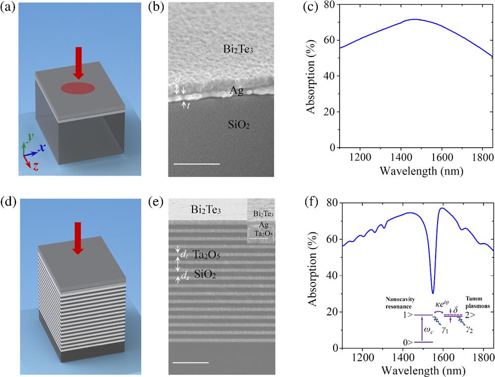
    Fig. 1. TI structures and absorption spectra. (a) 3D diagram of the ultrathin nanocavity with a TI nanofilm coated on a metallic layer. (b) Angle-tilted cross-sectional SEM image of a Bi2Te3 TI nanocavity deposited on a SiO2 substrate. The scale bar is 200 nm. Here, d and t are the thicknesses of Bi2Te3 and silver nanofilms, respectively. (c) Experimental measurement of the absorption spectrum of the nanocavity with a 42-nm Bi2Te3 film on a 30-nm silver layer (i.e., d=42  nm and t=30  nm). (d) 3D diagram of a TI nanocavity on a 1D photonic crystal. (e) Cross-sectional SEM image of a Bi2Te3 nanocavity on a photonic crystal with alternately stacked Ta2O5 and SiO2 layers. Here, dt and ds are the thicknesses of Ta2O5 and SiO2 layers, respectively. N is the periodic number. The scale bar is 2  μm. The inset shows the high-resolution SEM image of Bi2Te3 and silver films on the photonic crystal. The scale bar is 200 nm. (f) Measured absorption spectrum of the TI nanocavity/photonic crystal structure with dt=182  nm, ds=260  nm, d=42  nm, t=30  nm, and N=16. The inset depicts a three-level system of the EIT-like effect. ωc stands for the nanocavity resonant frequency. δ is the frequency detuning between the nanocavity resonance and Tamm plasmons in silver/photonic crystal structure. γ1 and γ2 are the decaying rates of nanocavity resonance and Tamm plasmons, respectively. κeiφ is the complex coupling coefficient between the nanocavity resonance and Tamm plasmons with a phase retardation φ.
    Material characterization and optical constants of Bi2Te3 TI. (a) TEM image of a grown 42-nm Bi2Te3 TI film transferred on the supporter of a copper microgrid. (b) SAED pattern of the Bi2Te3 nanofilm. (c) HRTEM image of the Bi2Te3 nanofilm. (d) Ellipsometer-measured (circles) and fitted (curves) refractive indices and extinction coefficients of Bi2Te3 TI at the wavelengths from 230 to 1930 nm. (e), (f) Fitted refractive indices and extinction coefficients of Bi2Te3 TI surface and bulk states with the layer-on-bulk model [the inset in panel (d)].
    Fig. 2. Material characterization and optical constants of Bi2Te3 TI. (a) TEM image of a grown 42-nm Bi2Te3 TI film transferred on the supporter of a copper microgrid. (b) SAED pattern of the Bi2Te3 nanofilm. (c) HRTEM image of the Bi2Te3 nanofilm. (d) Ellipsometer-measured (circles) and fitted (curves) refractive indices and extinction coefficients of Bi2Te3 TI at the wavelengths from 230 to 1930 nm. (e), (f) Fitted refractive indices and extinction coefficients of Bi2Te3 TI surface and bulk states with the layer-on-bulk model [the inset in panel (d)].
    TI thickness-dependent nanocavity resonance and induced transparency. (a) Experimentally measured absorption spectra of the TI nanocavities on the SiO2 substrate with different Bi2Te3 film thicknesses d when t=30 nm. (b) Corresponding resonance wavelengths of the TI nanocavity with different d. The curve, red circles, and blue circles denote the theoretical, experimental, and simulation results, respectively. (c) Corresponding magnetic field distribution of the TI nanocavity with a 42-nm Bi2Te3 film (i.e., d=42 nm) at the absorption peak wavelength. (d), (e) Measured and simulated absorption spectra of the TI nanocavity/photonic crystal structures with different d when t=30 nm. (f) Corresponding magnetic field distribution of the TI nanocavity/photonic crystal structure with a 42-nm Bi2Te3 film at the absorption dip wavelength.
    Fig. 3. TI thickness-dependent nanocavity resonance and induced transparency. (a) Experimentally measured absorption spectra of the TI nanocavities on the SiO2 substrate with different Bi2Te3 film thicknesses d when t=30  nm. (b) Corresponding resonance wavelengths of the TI nanocavity with different d. The curve, red circles, and blue circles denote the theoretical, experimental, and simulation results, respectively. (c) Corresponding magnetic field distribution of the TI nanocavity with a 42-nm Bi2Te3 film (i.e., d=42  nm) at the absorption peak wavelength. (d), (e) Measured and simulated absorption spectra of the TI nanocavity/photonic crystal structures with different d when t=30  nm. (f) Corresponding magnetic field distribution of the TI nanocavity/photonic crystal structure with a 42-nm Bi2Te3 film at the absorption dip wavelength.
    EIT-like response with different silver film thicknesses. (a) Theoretical evolution of absorption spectrum from the TI nanocavity/photonic crystal structures with different silver film thicknesses t when d=44 nm. (b) Measured (solid curves) and fitted (dashed curves) absorption spectra of the TI nanocavity/photonic crystal structures with different t when d=44 nm. Here, the experimentally measured spectra were fitted with the TCO model. (c) Fitted decaying rates γ2 and coupling strengths κ in the TCO model with different t. The inset shows the corresponding decaying rates γ1.
    Fig. 4. EIT-like response with different silver film thicknesses. (a) Theoretical evolution of absorption spectrum from the TI nanocavity/photonic crystal structures with different silver film thicknesses t when d=44  nm. (b) Measured (solid curves) and fitted (dashed curves) absorption spectra of the TI nanocavity/photonic crystal structures with different t when d=44  nm. Here, the experimentally measured spectra were fitted with the TCO model. (c) Fitted decaying rates γ2 and coupling strengths κ in the TCO model with different t. The inset shows the corresponding decaying rates γ1.
    Hua Lu, Shouhao Shi, Dikun Li, Shuwen Bo, Jianxu Zhao, Dong Mao, Jianlin Zhao. λ/20-Thick cavity for mimicking electromagnetically induced transparency at telecommunication wavelengths[J]. Advanced Photonics, 2024, 6(3): 036001
    Download Citation