Abstract
1. INTRODUCTION
High-speed electro-optic (EO) modulators are key components in high-capacity, reconfigurable, and intelligent optical systems [1–6]. Recently, thin-film lithium-niobate-on-insulator (LNOI) systems with high EO coefficients have regained intensive interest for high-speed modulation because they offer high refractive-index contrast and possible compatibility with the complementary-metal-oxide-semiconductor (CMOS) processes [7,8]. High-performance EO modulators on LNOI have been demonstrated with the advantages of low losses, high bandwidths, and high linearity [9–12]. Currently, the demonstrated modulators on LNOI are mainly realized with a Mach–Zehnder interferometer (MZI) or a ring resonator. When using MZIs, which utilize two-beam interference [13,14], the footprint is usually as large as several centimeters. In order to achieve compact optical modulators, ring resonators are preferred [15–17]. However, for an - or -cut LNOI wafer with excellent EO modulation, the waveguide bending radius should be as large as hundreds of micrometers to suppress mode hybridization due to the large LN anisotropy [18–20]. Therefore, a ring-resonator-based EO modulator usually occupies a large footprint on the platform of LNOI. Alternatively, a Fabry–Perot (FP) resonator, which has no waveguide bends, is a very promising candidate for achieving ultracompact EO modulators. Unfortunately, for a traditional FP resonator, modulated light is reflected back to the input port [21,22], and thus an external isolator or circulator is usually required to avoid disturbing the transmission system.
In this paper, we propose and demonstrate an ultracompact and high-speed EO modulator using a new FP cavity on an LNOI platform. The proposed FP cavity is constructed by a pair of mirrors based on asymmetric multimode waveguide gratings (AMWGs). Here the AMWGs are designed so that the forward () mode is reflected into the backward () mode [23,24]. In this way, the reflected and incident paths can then be separated with the assistance of a mode (de)multiplexer. The demonstrated modulator exhibits a low excess loss (EL) of and a high extinction ratio (ER) of . The eye diagrams of 40 Gbps on–off keying (OOK) and 80 Gbps 4-pulse amplitude modulation (PAM4) signals with excellent quality are demonstrated. Such an electro-optic FP cavity can also be used as ultrafast optical switches.
2. STRUCTURE AND DESIGN
Figure 1(a) shows the schematic configuration of the proposed EO modulator using a new FP cavity on an LNOI platform. Here the FP cavity is formed by a pair of AMWG mirrors connected with mode (de)multiplexers based on adiabatic dual-core taper. The AMWGs are introduced to partially reflect the forward () mode into the backward () mode when the wavelength is around the Bragg wavelength. Thus, there are two guided modes propagating in the opposite directions in the FP cavity. When the mode launches at input port #1, one has a high transmission of the mode at port #3 for the wavelength within the resonance-wavelength band of the FP cavity. Meanwhile, there is a high transmission of the mode at port #4 for the wavelength beyond the resonance-wavelength band of the FP cavity because the reflected/converted mode by the AMWG is finally converted to the mode at port #4 by the mode (de)multiplexer. Similarly, when the mode launches at input port #2, the transmissions at port #3 and at port #4 are similar to and , respectively. When the ground-signal electrodes are applied with electrical signals, the lateral electric field is generated, and thus the refractive index of LN is modified very fast due to the Pockels effect. As a result, the resonant wavelength of the FP cavity has some shift, resulting in a high-speed modulation.
Sign up for Photonics Research TOC. Get the latest issue of Photonics Research delivered right to you!Sign up now
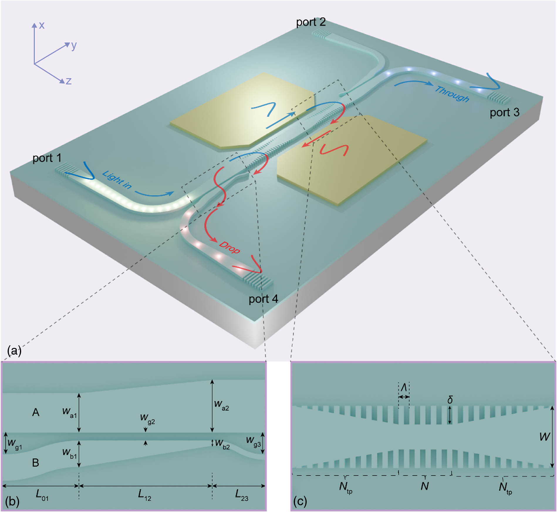
Figure 1.(a) Schematic configuration of the proposed ultracompact and high-speed EO modulator using a new
In this design, the waveguide structure is patterned on an -cut 400 nm thick LNOI with an etching depth of 200 nm and an air upper-cladding. Here the wavelength is around 1550 nm, and one has and for the LN material. For the mode (de)multiplexers, the adiabatic dual-core taper coupler shown in Fig. 1(b) is designed according to the method proposed in our previous work [25]. The core widths at the input ends of waveguides A and B are chosen to be different (e.g., ) so that the two lowest-order supermodes supported by the dual-core waveguide are localized in the two core regions. In contrast, the core widths at the output ends of waveguides A and B are chosen to be very different (e.g., ) so that the two lowest-order supermodes can be localized in the wide core region. When waveguides A and B are tapered adiabatically, one can (de)multiplex the and modes with low excess loss and low cross talk in a broad wavelength band. We choose the core widths at the input/output ends of waveguides A and B for the adiabatic coupler as and , respectively. With this design, the core width of waveguide A increases from 1.0 to 2.0 μm, while the core width of waveguide B decreases from 0.6 to 0.2 μm. The taper lengths are chosen as while the gap widths are chosen as .
For the AMWG, the structure is designed according to the phase-matching condition between the mode and the mode [26], so that the () mode launched at the input port can be converted into the reflected () mode. The phase-matching condition for the mode conversion in the grating is given as , where and are the effective refractive indices of the and modes in the AMWG waveguide, respectively, is the grating period, and is the Bragg wavelength. In order to suppress the undesired reflection loss at the front/back ends of the grating section, here we introduce grating tapers to connect the waveguide and grating sections as shown in Fig. 1(c). The corrugation depth is varied linearly from the minimum to the maximum in the grating taper, and the taper length should be long enough to be adiabatic. One has , where is the number of the period in the taper section. When is confirmed, the reflectivity of AMWG can vary by adjusting the number of the period in the middle section [see Fig. 1(c)]. In this paper, the designed AMWG has the following parameters: the period , the period number , the period number , the corrugation depth , and the core width . The length of the straight section between the two AMWGs is 10 μm, while the corresponding equivalent cavity length is about 60 μm, considering the average reflection point of AMWGs. As a result, here the electrode length is chosen to 80 μm to achieve sufficient modulation efficiency, while the gap between the two electrodes is set to 5 μm in order to avoid the metal absorption loss. Note that, for a regular MZI modulator, the length is usually larger than the wavelength of the supported microwave, and thus the traveling microwave is required to have the same traveling speed (also known as the same group refractive index) as the light wave for maximizing the modulation efficiency. In contrast, the feature size of electrodes in the present FP-cavity-based modulator is much smaller than the microwave wavelength. In this case the electrodes can be considered by a lumped model, which does not involve a traveling microwave and thus it is not required to match the group refractive indices of the light wave and microwave. For the designed FP cavity, the total footprint is as compact as .
Figure 2(a) shows the simulated transmissions when the and modes are launched at the input side of waveguide A, indicating that the launched mode is bounded in waveguide A with a low loss () and low cross talk of coupled into waveguide B, while the mode is coupled from waveguide A to waveguide B very efficiently with a low loss of . Figure 2(b) shows the simulated light propagation in the designed mode (de)multiplexers when operating at the central wavelength 1550 nm for the launched and modes. It can be seen that the mode launched from the right side of waveguide A can be converted efficiently to the mode at the left side of waveguide B, while the mode launched from the right side of waveguide A can be transmitted directly to the left side. The calculated transmission and reflection of the AMWG for the launched mode are shown in Fig. 2(c), indicating that the reflection is as high as when operating around 1550 nm. Figure 2(d) shows the simulated light propagation in the designed AMWG when operating at the wavelengths of 1550 nm and 1600 nm. It can be seen that the mode transmits through the AMWG directly at 1600 nm, while the mode is reflected at 1550 nm.
Figure 2.(a) Calculated transmissions from the
3. FABRICATION AND MEASUREMENT
The devices were then fabricated with an -cut LNOI wafer from NANOLN, and the nominal thickness of the LN layer is 400 nm. The device structure was first patterned by using an electron-beam lithography (EBL) process, and the LN layer was then etched by plasma. The electrodes were then formed with a lift-off process, and the thicknesses of the titanium and gold electrodes are 10 nm and 150 nm, respectively. The fabricated FP-cavity modulator is shown in Fig. 3(a). Figures 3(b)–3(d) show the scanning electron microscope (SEM) images for the dual-core taper of the mode (de)multiplexer, the modulation region, as well as the AMWG. For the LNOI waveguide, the sidewall angle is usually about 30° (relative to the vertical axis), while the sidewall angle decreases to about 22° in the nanoslots of AMWG due to the proximity effect.
Figure 3.(a) The optical microscope image of the fabricated FP cavity modulator based on AMWGs; the SEM images of (b) the dual-core taper of mode (de)multiplexer, (c) the modulation region, and (d) the AMWG.
Grating couplers for TE polarization were used to achieve efficient chip-fiber coupling for the convenience of measurement, and the grating coupler has a high coupling efficiency of . A broadband amplified spontaneous emission (ASE) light source was used as the source, and an optical spectrum analyzer (OSA) was applied to read out the output response. The measured results were normalized with respect to the transmission of a 1 μm wide straight waveguide connected with grating couplers on the same chip. Figures 4(a) and 4(b) show the measured transmissions and of the presented EO modulator, showing the resonant peak around 1536 nm. It can also be seen that the transmissions and are almost the same. The fabricated EO modulator exhibits a low excess loss of , a high extinction ratio of , and a loaded factor of . Here the excess loss refers to the power difference between the transmitted resonance peak power at the through port and the transmission from a straight waveguide on the same chip. The DC voltage from a source meter was applied to the metal electrodes for measuring the static electro-optic response. Figures 4(c) and 4(d) show the measured transmissions and when applying different voltages of , , 0, 10, and 20 V, respectively. It can be seen that the modulation efficiency is about 7 pm/V, and the modulations at the through and drop ports are respectively about 7 dB and 10 dB by applying a voltage of 20 V.
Figure 4.Measured transmissions (a)
Figures 5(a) and 5(b) show the measured small-signal EO response () of the fabricated EO modulator for the transmissions and . Here a vector network analyzer (VNA) was used to generate and receive RF signals. The input light from a tunable laser with polarization controlled by a fiber polarization controller (PC) was coupled into the LN chip through a grating coupler. The wavelength was set around the resonance. In order to achieve the wavelength alignment, it is possible to apply a DC bias for a fine wavelength tuning. Alternatively, it is also possible to add a micro-heater to tune the wavelength thermally. The input light was modulated through the amplified RF signal and then coupled out of chip through a grating coupler. Finally, the modulated light was amplified by an erbium-doped fiber amplifier (EDFA), filtered by a bandpass filter (BPF), then detected by a 70 GHz photodetector (PD). The optical wavelength was detuned to have the highest slope around the resonance at 1536 nm. From Figs. 5(a) and 5(b), it can be seen that the measured 3 dB EO bandwidth of the fabricated modulator is about 25 GHz, which is close to the photon-lifetime-limited bandwidth estimated from the measured factor with the formula of , where is the optical frequency and is the quality factor [27,28]. The modulation bandwidth is mainly limited by RC time of the electrodes and the photon lifetime of the FP cavity. For the present devices, the electrodes have quite small resistance and capacitance, and the RC-limited modulation bandwidth is . On the other hand, for the present FP cavity with a factor of , the photon-lifetime-limited modulation bandwidth is . As a result, we conclude that the photon lifetime gives the upper limit of the modulation bandwidth.
Figure 5.Measured small-signal EO response (
Finally, high-speed digital data transmission of the fabricated EO modulator was characterized experimentally. Here an arbitrary wave generator (AWG) connected to the clock source was used to generate the pseudo-random bit sequence (PRBS), and a 55 GHz RF amplifier was used to amplify the driving signal. The modulated light was then collected by a wide-bandwidth oscilloscope (WBO). Figures 6(a) and 6(b) show the measured eye diagrams for the OOK signal at the data rate of 40 Gbps and the PAM4 signal at the data rate of 80 Gbps for the transmissions and , respectively. It can be seen that the eyes are well open with excellent quality. With the driving peak-to-peak voltage of , the extinction ratio of the eye diagrams is . Numerical simulations show that the present modulator exhibits a small capacitance of , and the energy consumption for the OOK signal is about 4.5 fJ/bit (given by [29]). Note that the trade-off between the bandwidth and the driving voltage indeed exists in LN modulators. There are some potential solutions to the challenge by, e.g., using a Fano resonance [30] or the coupling modulation (instead of resonance-wavelength shifting) [31].
Figure 6.Measured eye diagrams for the OOK signal at the data rate of 40 Gbps and the PAM4 signal at the data rate of 80 Gbps for the transmissions (a)
4. CONCLUSION
To conclude, we have proposed and demonstrated a high-speed LNOI electro-optic modulator based on a new FP cavity. This FP cavity consists of a pair of AMWG mirrors, which are designed to reflect the forward () mode to the backward () mode. The reflected and incident paths can then be separated with the assistance of a mode (de)multiplexer. The present modulator exhibits a low excess loss of and a high extinction ratio of , as well as a compact footprint of . For the demonstrated modulator, the electro-optic modulation efficiency is about 7 pm/V, and the 3 dB bandwidth is about 25 GHz, enabling high-speed modulation of up to 40 Gbps for OOK signals and 80 Gbps for PAM4 signals. Such an EO modulator is promising to many applications in multidisciplinary areas like data transmission, signal processing, and beam steering, and so on. Furthermore, the present electro-optic FP cavity is also useful as an ultrafast optical switch and can be scalable for large-scale optical switch arrays.
References
[1] C. Haffner, D. Chelladurai, Y. Fedoryshyn, A. Josten, B. Baeuerle, W. Heni, T. Watanabe, T. Cui, B. Cheng, S. Saha, D. L. Elder, L. R. Dalton, A. Boltasseva, V. M. Shalaev, N. Kinsey, J. Leuthold. Low-loss plasmon-assisted electro-optic modulator. Nature, 556, 483-486(2018).
[2] C. T. Phare, Y.-H. D. Lee, J. Cardenas, M. Lipson. Graphene electro-optic modulator with 30 GHz bandwidth. Nat. Photonics, 9, 511-514(2015).
[3] J.-H. Han, F. Boeuf, J. Fujikata, S. Takahashi, S. Takagi, M. Takenaka. Efficient low-loss InGaAsP/Si hybrid MOS optical modulator. Nat. Photonics, 11, 486-490(2017).
[4] M. Lee, H. E. Katz, C. Erben, D. M. Gill, P. Gopalan, J. D. Heber, D. J. McGee. Broadband modulation of light by using an electro-optic polymer. Science, 298, 1401-1403(2002).
[5] L. Alloatti, R. Palmer, S. Diebold, K. P. Pahl, B. Chen, R. Dinu, M. Fournier, J.-M. Fedeli, T. Zwick, W. Freude, C. Koos, J. Leuthold. 100 GHz silicon–organic hybrid modulator. Light Sci. Appl., 3, e173(2014).
[6] A. Honardoost, R. Safian, M. Teng, L. Zhuang. Ultralow-power polymer electro–optic integrated modulators. J. Semicond., 40, 070401(2019).
[7] A. Boes, B. Corcoran, L. Chang, J. Bowers, A. Mitchell. Status and potential of lithium niobate on insulator (LNOI) for photonic integrated circuits. Laser Photon. Rev., 12, 1700256(2018).
[8] S. Yuan, C. Hu, A. Pan, Y. Ding, X. Wang, Z. Qu, J. Wei, Y. Liu, C. Zeng, J. Xia. Photonic devices based on thin-film lithium niobate on insulator. J. Semicond., 42, 041304(2021).
[9] B. Pan, J. Hu, Y. Huang, L. Song, J. Wang, P. Chen, Z. Yu, L. Liu, D. Dai. Demonstration of high-speed thin-film lithium-niobate-on-insulator optical modulators at the 2-μm wavelength. Opt. Express, 29, 17710-17717(2021).
[10] C. Wang, M. Zhang, X. Chen, M. Bertrand, A. Shams-Ansari, S. Chandrasekhar, P. Winzer, M. Lončar. Integrated lithium niobate electro-optic modulators operating at CMOS-compatible voltages. Nature, 562, 101-104(2018).
[11] P. Kharel, C. Reimer, K. Luke, L. He, M. Zhang. Breaking voltage–bandwidth limits in integrated lithium niobate modulators using micro-structured electrodes. Optica, 8, 357-363(2021).
[12] M. He, M. Xu, Y. Ren, J. Jian, Z. Ruan, Y. Xu, S. Gao, S. Sun, X. Wen, L. Zhou, L. Liu, C. Guo, H. Chen, S. Yu, L. Liu, X. Cai. High-performance hybrid silicon and lithium niobate Mach–Zehnder modulators for 100 Gbits-1 and beyond. Nat. Photonics, 13, 359-364(2019).
[13] S. Wang, D. Dai. Polarization-insensitive 2 × 2 thermo-optic Mach–Zehnder switch on silicon. Opt. Lett., 43, 2531-2534(2018).
[14] L. Song, H. Li, D. Dai. Mach–Zehnder silicon-photonic switch with low random phase errors. Opt. Lett., 46, 78-81(2021).
[15] C. Zhang, M. Zhang, Y. Xie, Y. Shi, R. Kumar, R. R. Panepucci, D. Dai. Wavelength-selective 2 × 2 optical switch based on a Ge2Sb2Te5-assisted microring. Photon. Res., 8, 1171-1176(2020).
[16] C. Wang, M. Zhang, B. Stern, M. Lipson, M. Lončar. Nanophotonic lithium niobate electro-optic modulators. Opt. Express, 26, 1547-1555(2018).
[17] D. Liu, J. Tang, Y. Meng, W. Li, N. Zhu, M. Li. Ultra-low
[18] B. Pan, Y. Tan, P. Chen, L. Liu, Y. Shi, D. Dai. Compact racetrack resonator on LiNbO3. J. Lightwave Technol., 39, 1770-1776(2021).
[19] J. Wang, P. Chen, D. Dai, L. Liu. Polarization coupling of
[20] A. Pan, C. Hu, C. Zeng, J. Xia. Fundamental mode hybridization in a thin film lithium niobate ridge waveguide. Opt. Express, 27, 35659-35669(2019).
[21] M. Xu, M. He, X. Liu, Y. Pan, S. Yu, X. Cai. Integrated lithium niobate modulator and frequency comb generator based on Fabry-Perot resonators. Conference on Lasers and Electro-Optics, JTh2B.27(2020).
[22] M. V. Kotlyar, S. Iadanza, L. O’Faolain. Lithium niobate Fabry-Perot microcavity based on strip loaded waveguides. Photon. Nanostruct. Fundam. Appl., 43, 100886(2021).
[23] D. Liu, D. Dai. Silicon-based polarization-insensitive optical filter with dual-gratings. Opt. Express, 27, 20704-20710(2019).
[24] D. Liu, H. Wu, D. Dai. Silicon multimode waveguide grating filter at 2 μm. J. Lightwave Technol., 37, 2217-2222(2019).
[25] D. Dai, C. Li, S. Wang, H. Wu, Y. Shi, Z. Wu, S. Gao, T. Dai, H. Yu, H.-K. Tsang. 10-channel mode (de)multiplexer with dual polarizations. Laser Photon. Rev., 12, 1700109(2018).
[26] H. Qiu, J. Jiang, T. Hu, P. Yu, J. Yang, X. Jiang, H. Yu. Silicon add-drop filter based on multimode Bragg sidewall gratings and adiabatic couplers. J. Lightwave Technol., 35, 1705-1709(2017).
[27] G. Li, X. Zheng, J. Yao, H. Thacker, I. Shubin, Y. Luo, K. Raj, J. E. Cunningham, A. V. Krishnamoorthy. 25 Gb/s 1 V-driving CMOS ring modulator with integrated thermal tuning. Opt. Express, 19, 20435-20443(2011).
[28] M. Li, J. Ling, Y. He, U. A. Javid, S. Xue, Q. Lin. Lithium niobate photonic-crystal electro-optic modulator. Nat. Commun., 11, 4123(2020).
[29] D. A. B. Miller. Attojoule optoelectronics for low-energy information processing and communications. J. Lightwave Technol., 35, 346-396(2017).
[30] B.-B. Li, Y.-F. Xiao, C.-L. Zou, X.-F. Jiang, Y.-C. Liu, F.-W. Sun, Y. Li, Q. Gong. Experimental controlling of Fano resonance in indirectly coupled whispering-gallery microresonators. Appl. Phys. Lett., 100, 021108(2012).
[31] W. D. Sacher, W. M. J. Green, S. Assefa, T. Barwicz, H. Pan, S. M. Shank, Y. A. Vlasov, J. K. S. Poon. Coupling modulation of microrings at rates beyond the linewidth limit. Opt. Express, 21, 9722-9733(2013).
Set citation alerts for the article
Please enter your email address