• Infrared and Laser Engineering
  • Vol. 51, Issue 2, 20210878 (2022)
Chunjie Feng1, Xiaobo Zhu1、*, Yanghui Wu1, Chen Fu1, Huiyu Chang1, Yutao Yue2, and Wenhua Gu1
Author Affiliations
  • 1School of Electronic and Optical Engineering, Nanjing University of Science and Technology, Nanjing 210094, China
  • 2Jiangsu Jicui Depth Perception Technology Research Institute Co., Ltd., Wuxi 214115, China
  • show less
    DOI: 10.3788/IRLA20210878 Cite this Article
    Chunjie Feng, Xiaobo Zhu, Yanghui Wu, Chen Fu, Huiyu Chang, Yutao Yue, Wenhua Gu. Application of electrostatic jet-print technology in terahertz metasurface devices fabrication[J]. Infrared and Laser Engineering, 2022, 51(2): 20210878 Copy Citation Text show less
    (a) Schematic diagram and (b) optical picture of the home-made electrostatic jet printing system based on EHD principle
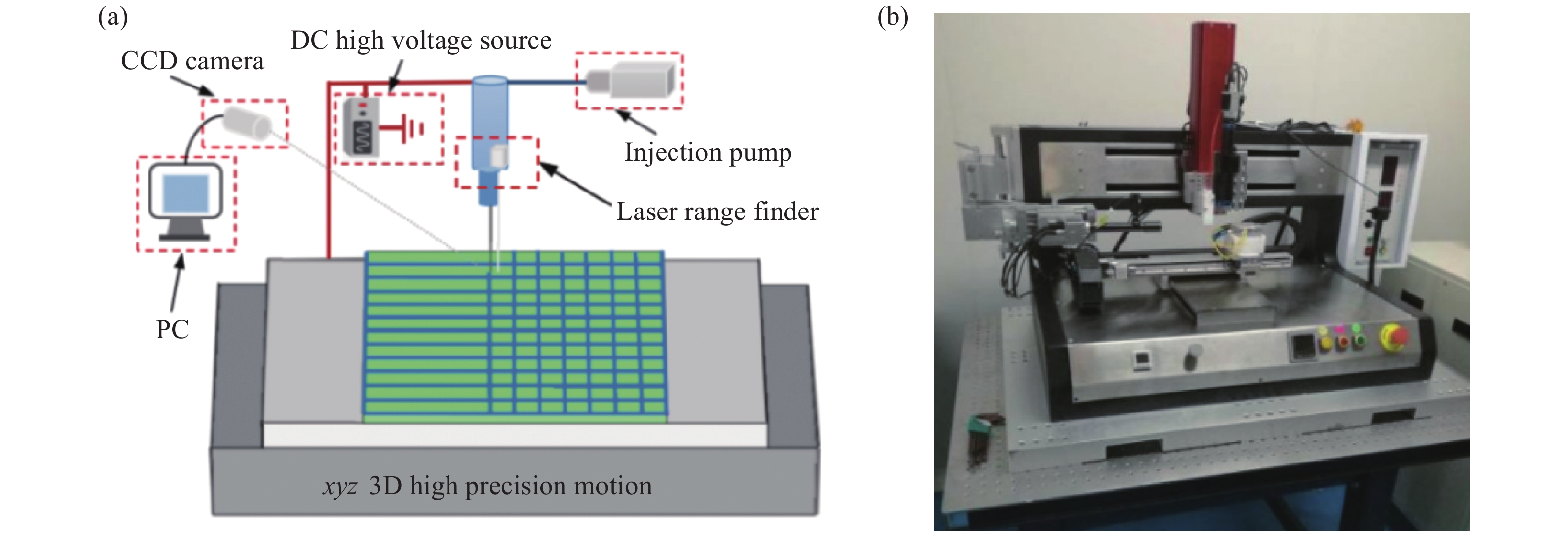
    Fig. 1. (a) Schematic diagram and (b) optical picture of the home-made electrostatic jet printing system based on EHD principle
    Picture of a nozzle with an internal diameter of 500 μm producing a jet with the diameter of 4.4 μm (Scale bar is 300 μm)
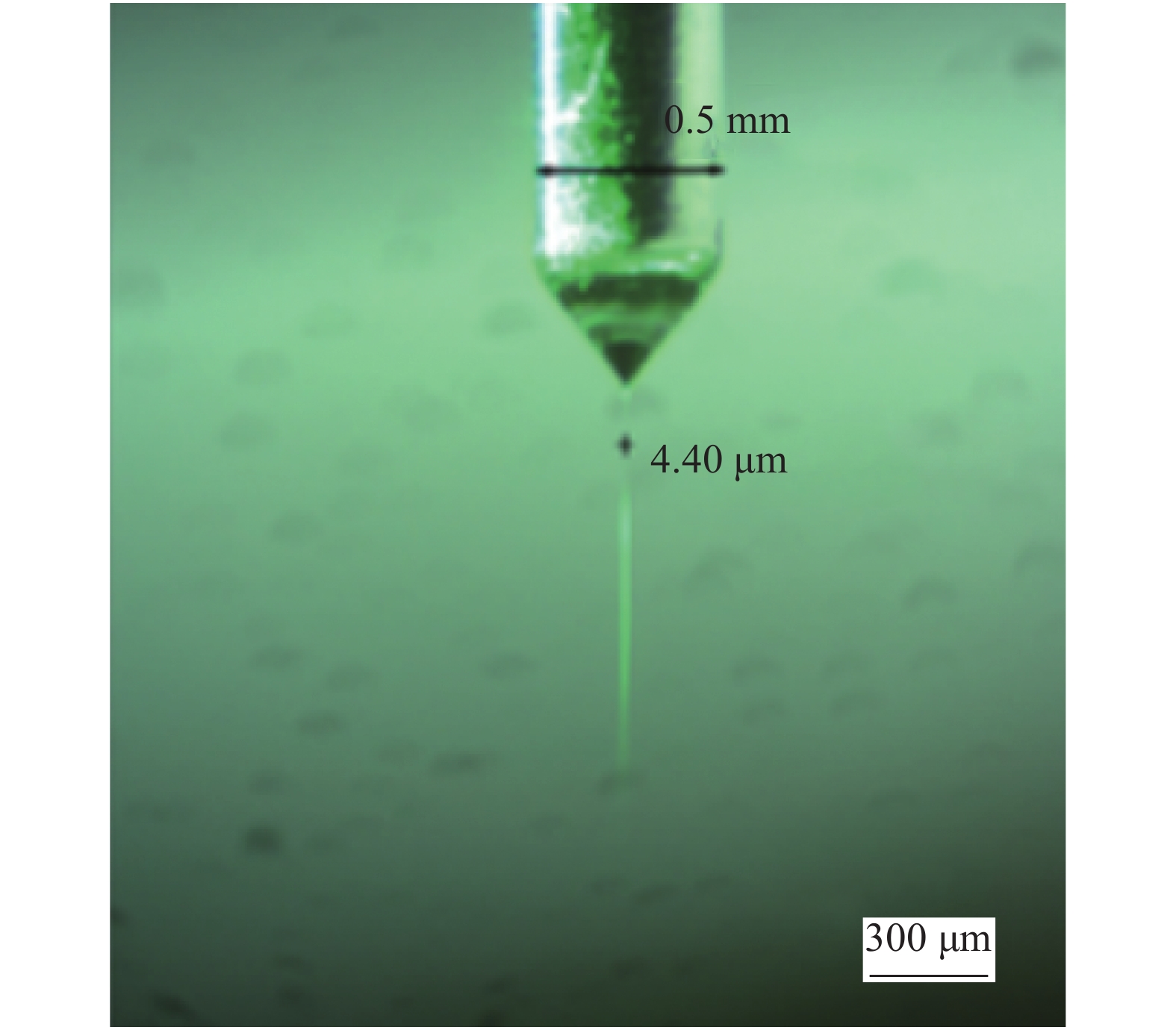
    Fig. 2. Picture of a nozzle with an internal diameter of 500 μm producing a jet with the diameter of 4.4 μm (Scale bar is 300 μm)
    (a) A transparent metal grid sample with the line width of about 5 μm on a glass substrate (the scale bar is 200 μm and 50 μm); (b) Visible light transmission spectrum of the sample
    Fig. 3. (a) A transparent metal grid sample with the line width of about 5 μm on a glass substrate (the scale bar is 200 μm and 50 μm); (b) Visible light transmission spectrum of the sample
    Complex patterns with discontinuous points printed on the glass substrate (Scale bar is 5 mm)
    Fig. 4. Complex patterns with discontinuous points printed on the glass substrate (Scale bar is 5 mm)
    Schematic of (a) structure and (b) equivalent circuit model of the multilayer terahertz absorber
    Fig. 5. Schematic of (a) structure and (b) equivalent circuit model of the multilayer terahertz absorber
    Absorption curves obtained by simulation, equivalent circuit calculation, and experimental results
    Fig. 6. Absorption curves obtained by simulation, equivalent circuit calculation, and experimental results
    Picture of the terahertz absorber sample indicating the good optical transparency (Scale bar is 400 μm)
    Fig. 7. Picture of the terahertz absorber sample indicating the good optical transparency (Scale bar is 400 μm)
    Schematic of (a) unit structure and (b) the top schematic view of a terahertz polarization converter
    Fig. 8. Schematic of (a) unit structure and (b) the top schematic view of a terahertz polarization converter
    (a) Co- and cross-polarized reflectance and (b) polarization conversion rate of the terahertz polarization converter
    Fig. 9. (a) Co- and cross-polarized reflectance and (b) polarization conversion rate of the terahertz polarization converter
    ParameterValue
    d1/μm 175
    d2/μm 175
    p/μm 400
    2a/μm 20
    Rs/Ω·sq−150
    h_Ag/μm 1
    Table 1. Optimized parameters of the terahertz absorber
    Chunjie Feng, Xiaobo Zhu, Yanghui Wu, Chen Fu, Huiyu Chang, Yutao Yue, Wenhua Gu. Application of electrostatic jet-print technology in terahertz metasurface devices fabrication[J]. Infrared and Laser Engineering, 2022, 51(2): 20210878
    Download Citation