
Zarko Sakotic, Alex Krasnok, Andrea Alú, Nikolina Jankovic, "Topological scattering singularities and embedded eigenstates for polarization control and sensing applications," Photonics Res. 9, 1310 (2021)
- Photonics Research
- Vol. 9, Issue 7, 1310 (2021)
Abstract
1. INTRODUCTION
Along with the progress in fabrication technologies observed in the last few decades, the concepts of metamaterials [1], metasurfaces [2], and photonic crystals [3] have brought forward a previously unattainable level of control of visible, infrared, and microwave electromagnetic waves. More recently, the pursuit of wave control has been expanded with tools borrowed from the field of topology [4], enabling phenomena such as robustness to imperfections and immunity to backscattering [5,6], as well as unidirectional transport [7]. Topological photonics has been rapidly growing in recent years, transferring established concepts from condensed-matter systems to electromagnetics research and metamaterials. Topological systems are usually quantified with an invariant—an integer-valued quantity, such as the Chern number [8], which does not change upon continuous deformations that preserve the topological nature [9]. Although topological aspects of photonic systems have mostly been driven through the condensed matter physics perspective, recently there has been an expansion of topological photonics beyond these boundaries, leveraging the distinct features of photons [10,11]. Contrary to the fermionic nature of electrons, photons have a bosonic nature, thus offering different opportunities for the realization of topological phenomena [12]. Specifically, topological effects are increasingly being found in scattering and radiative processes [13], moving beyond the limitations of the tight-binding model that commonly models electronic systems [11]. Bound states in the continuum (BICs) or embedded eigenstates (EEs), examples of peculiar features associated with electromagnetic radiation and scattering, provide topological features for the optical response rooted in modes that are non-radiative yet embedded within the radiation continuum [14–21].
Photonic EEs supported by periodic systems have indeed been shown to possess topological features in the form of a polarization singularity in the wave vector space. Their robustness has been explicitly attributed to their topological nature [22,23], rooted in the fact that these singularities comply with topological charge conservation [24,25]. The topological nature of EEs has spun-off several research efforts, exploring the merging of EE charges to produce even more confined resonances in realistic systems [26] and unidirectional guided modes within the continuum [27]. The topological properties of EEs have been especially useful for polarization control, as it was shown that topologically protected polarization conversion is possible [28–30], and circularly polarized states can arise from BICs by breaking spatial symmetries [31–33]. Recently, the generation of vortex beams through EEs [34] and efficient topological vortex laser generation [35] were demonstrated, showing the potential of topological phenomena in radiative and scattering processes. Further connection between novel topological phenomena in the form of higher-order corner states and EEs has also recently been established in Ref. [11], indicating the far-reaching topological consequences that non-radiating states may have on the topological states of electromagnetic structures. Besides using the standard Hamiltonian formalism, the topological features of these systems can be studied through the scattering matrix formalism, and specifically by analyzing the complex reflection coefficient, where phase vortices arise [28,36,37]. This approach is very valuable because the features of the scattering matrix correspond to actual observables that can be looked for experimentally.
Although the topological aspects of EE-related phenomena are well understood in periodic systems, there has been little exploration into the topological features of other photonic systems that support EEs. Specifically, EEs arising in structures with singular values of the permittivity, mainly using epsilon-near-zero (ENZ) materials, have been recently studied [38–41], showing that they enable versatile optical and thermal emission properties [42,43]. However, their topological nature has not been discussed yet, which may further boost their potential in photonic and thermal applications. Furthermore, scattering anomalies such as EEs can be well studied in the complex frequency plane [44], which has not been applied so far to the analysis of topological scattering phenomena.
Sign up for Photonics Research TOC. Get the latest issue of Photonics Research delivered right to you!Sign up now
In this paper, we extend the concept of topological photonics to planar reflective systems that support EEs and, using the scattering matrix formalism and complex frequency analysis, we unveil their topological nature and the emergence of topologically protected scattering singularities. The proposed system supports symmetry-protected and accidental EEs, which are shown to be the origin of scattering singularities emerging upon insertion of loss/gain in the constituent materials. We focus on the lossy case and show that perfect-absorption singularities are intrinsically connected to the underlying EEs. Methods of formation, annihilation, and control of these topological charges are discussed, providing a versatile tool to manipulate amplitude, phase, and polarization of reflected waves. Using these concepts, we demonstrate several applications of these phenomena for polarization control and sensing.
2. RESULTS
A. Symmetry-Protected Embedded Eigenstates and Emerging Singularities
We consider a basic planar structure, infinitely extended in two dimensions as shown in Fig. 1(a) (left panel) and analyze the leaky mode dispersion of a perfect electric conductor (PEC)-backed slab with Drude permittivity dispersion
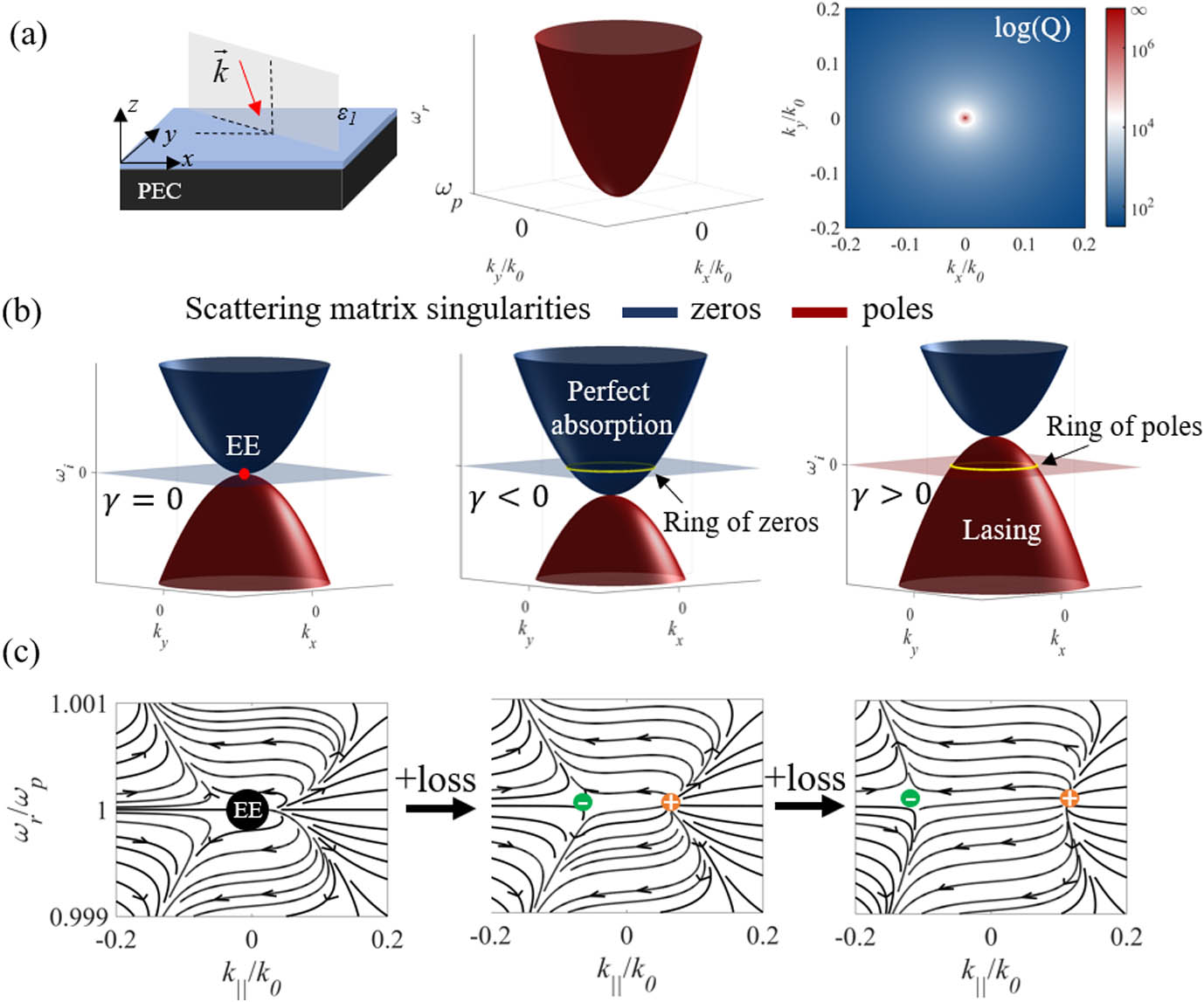
Figure 1.(a) Sketch of a PEC-backed slab with Drude dispersion; bulk mode dispersion for TM-polarized light. At
Namely, for zero transverse wavenumber
In order to obtain a better picture of the leaky nature of these modes in this basic geometry, we analyze the problem in the complex frequency space
Since the structure under consideration is backed by a PEC, it can be described by a one-port network, whose scattering matrix has only one element: the reflection coefficient,
Figure 1(b) shows the dispersion of the poles and zeros (red and blue) of
These types of vortices have been studied extensively in the context of singular optics [49,50]. The splitting of EE into a pair of charges, in this case a pair of perfectly absorbing points, sheds a new outlook to previous reports on pairs of perfect absorption occurring in reflective systems [36,51,52]. As we show later, each one of the analyzed EEs produces exactly two charges on the
B. Accidental EEs, Creation and Annihilation of Topological Charges, and Their Phase Signatures
To further enrich the discussion, we move to a more general scenario and analyze the system shown in Fig. 2(a), consisting of a dielectric spacer sandwiched between a PEC and a resonant top layer. We model the top layer with a Lorentz type of permittivity response, as shown in Fig. 2(b):
![]()
Figure 2.(a) Sketch of the planar multilayer structure under oblique illumination. (b) Permittivity dispersion of the top layer. (c), (d) Reflection-zero dispersion in the ENZ and ENP regions. For the ENZ case, thicknesses were chosen as
The spectral points of particular interest are the Lorentz resonance frequency
The dielectric spacer supports a continuum of modes above the light line, which couple to free-space radiation, as this structure is electromagnetically open from the top. However, if a mode of the spacer, i.e., a Fabry–Perot mode, overlaps with one of the top layer material resonances, a leaky mode with zero radiation decay (EE) is supported [38]. At
We first focus on the ENZ case. Figure 2(c) shows the dispersion of the reflection-zeros in
Although the magnitude of the reflection coefficient is unity for any frequency and angle in the lossless case, the EEs are visible in the reflection coefficient phase. In real–frequency space, they manifest themselves as phase resonances with diverging linewidth, as visible in Fig. 2(f). These features are only available for TM excitation due to the plasmonic nature of the underlying modes. A similar result with diverging phase resonances was reported in Ref. [56], although the origin of EE here is quite different.
The utility of phase analysis becomes apparent when losses are introduced; see Figs. 2(c) and 2(f)–2(h). Namely, the dispersion of reflection-zeros shown in Fig. 2(c) shifts down along the imaginary frequency axis, creating intersections with the
As shown in the amplitude plot, pairs of reflection-zeros and consequently perfect absorption points emerge from EE, where the charge emerging from the symmetry-protected EE has a mirror copy in the negative
A similar scenario arises for the ENP case. An accidental EE appears at a designed angle of 45°. More interestingly, however, both TM and TE modes have real-eigenfrequencies at the same point in the dispersion diagram; see Figs. 2(d) and 2(e). This happens because at
To verify the conservation of topological charge, we introduce a mechanism to annihilate charges. As evident from the reflection-zero dispersion diagrams in Figs. 2(c)–2(e), non-zero loss
Figure 3 shows the ENZ and ENP cases for TM-polarized light with reduced top-layer thickness. Comparing these results to Figs. 2(g), 2(h) and 2(j), 2(k), the neighboring charges have been annihilated and consequently the reflection-zeros associated with them have vanished. A useful rule-of-thumb can be inferred here: the angles at which EEs arise represent vertical walls impenetrable to these charges, and charges can move and annihilate only with the ones originating from neighboring EEs. For example, the remaining charge in the ENZ case in Figs. 3(a) and 3(b) cannot be destroyed for any level of material loss and thickness. Although there is a mirror copy of this charge in the negative
![]()
Figure 3.Charge annihilation for the lossy structures (
This result opens the question of material loss. Indeed, some of the naturally occurring materials have high absorption loss and, consequently, some features discussed here are not available, i.e., charges may already be destroyed due to large loss. However, if we constrain the discussion to low-loss or moderately lossy materials, e.g., polar dielectrics such as SiC, all of the previously described aspects hold. Furthermore, artificial materials as well as 2D materials, can provide ENZ or ENP response in different frequency regimes, thus expanding the validity of the presented analysis to a wide range of realistic geometries. For example, a Lorentzian (ENP) response can be induced as an electric dipole resonance in metasurfaces [36,51] or graphene strips [57], where similar features have been observed. In addition, an ENZ response can also be induced in the optical regime [58].
It is worth noting that the accidental EE at the designed angle
This is in contrast to EEs in photonic crystals, where accidental EEs arise at isolated
The discussion here adds new insights on previous observations of phase singularities and perfect absorption in metasurfaces [36], establishing a connection between topologically protected scattering features and EEs, and showing that properly designed planar structures can host a variety of topological scattering phenomena. The interplay of material and radiation losses provides control of the singularities and enables a versatile platform for the control of intensity and phase in reflection, which is important in applications such as thermal engineering, polarization control, and sensing.
C. Topological Charges near EE for Polarization Control
So far, our discussion has been constrained to the analysis of phase and amplitude of the reflection coefficient around EEs. However, an important aspect intrinsically connected to these features is polarization. Traditionally, manipulation of the polarization state of light has been based on wave plates [59]. When light propagates through birefringent crystals, orthogonal linear polarizations (LPs) experience different absorption coefficients and phase accumulation, enabling the generation of purely horizontal, vertical, or circular polarization (CP) at the output.
As we have shown in the previous discussion, the system of Fig. 2 displays co-located EEs with TE and TM polarization in the ENP case, and after accounting for loss, reflection-zeros of both polarizations emerge in the vicinity of each other. This property has interesting consequences for polarization control, as the two orthogonal polarization states experience dramatically different absorption coefficients and phase accumulation in the region containing these charges, allowing for different linear transformations of the polarization state upon reflection. To test the potential of this property, we use isotropic SiC to model the top-layer permittivity [60]. We choose
We plot the ellipsometric parameter
![]()
Figure 4.Polarization manipulation. (a) Ellipsometric parameter
To illustrate the opportunities for polarization control, we plot the total reflectance and the contour lines with specific
In order to better visualize this effect, we plot the output polarization ellipses for both CP and 45° LP inputs; see Figs. 4(c) and 4(d). Singular phase points produce purely vertical or horizontal polarization states in the output. This can be done efficiently since most of the desired polarization is reflected, while the other is fully absorbed. However, extracting horizontal or vertical polarization from a 45° LP or CP input is limited to 50% in efficiency, as no conversion from one to the other happens,
D. Singular Phase and Near-Annihilation Point for Sensing Applications
Phase vortices are characterized by an undefined phase point in their center, around which the phase changes dramatically. This feature, most commonly observable around reflection-zeros, has been used as a basis for interferometric phase sensing schemes [64–69]. Namely, even small changes in the environment can result in giant phase changes, thus creating one of the most sensitive schemes. Various systems exhibit these types of singular points, including metasurfaces [64], 1D photonic crystals [65], hyperbolic [66] and 2D materials [67]. Instead of using a traditional interferometric setup, most of these schemes use ellipsometric measurements, which measure phase and amplitude differences between orthogonal linear polarization components.
The caveat of this sensing method is the following: by approaching the singular point of the vortex, the phase changes more dramatically, thus increasing the sensitivity of the system. However, the amplitude of the reflection coefficient drops at the same time. The sensitivity diverges as the singular point is reached, but there is no reflection to be measured at the detector. This inverse relationship between sensitivity and
There are indeed qualitative differences between different realizations. Engineering structures with lower possible values of
To address these issues, we exploit the unusual physics around the EE and the related topological charges discussed in this paper. First, we show that using EEs in SiC provides high-
To achieve these goals, we envision a gold-backed air gap (spacer) covered by a SiC layer to be used as a trace gas sensor, operating at long-wave infrared wavelengths [Fig. 5(a)]. Gold is highly reflective at long-wave IR wavelengths; thus, it can work as an efficient reflective bottom layer. For the chosen gap size
![]()
Figure 5.(a) Sensing scheme based on phase singularities. (b) Phase of the reflection coefficient as the frequency is changed and passes near the vortex. Inset:
As shown in the previous discussion, the SiC-capped resonator can support an EE around 10.3 μm (ENZ region) and the accompanying reflection-zeros. To demonstrate the phase jump, we plot the reflection coefficient near EE and its phase as it passes near the vortex at 52.3° [Fig. 5(b)]. Based on this phase jump, we can detect tiny changes in the sensing layer, as indicated in the bottom left inset in Fig. 5(b). At a constant frequency and angle, the phase of reflected waves changes dramatically for permittivity changes of the order of
However, the displayed increase in sensitivity requires resolving the incidence angle in the order of 0.01°. For the DBR structure displayed in Fig. 5(c), the sensitivity drops by 1 order of magnitude with the angle changing by just 0.02°; see Fig. 6(a). Although the presented system has superior sensitivity, it suffers from the same drawback as in Ref. [67], as sensitivity is exceptionally dependent on the chosen incidence angle. This may result in unreliable sensitivity values, as most instruments cannot resolve at that level of precision.
![]()
Figure 6.Sensitivity of the reflection coefficient and sensitivity for different incidence angles. (a) The reflection coefficient of the DBR structure in Fig.
To alleviate this stringent requirement, we exploit the phenomenon of merging charges introduced above. Interestingly, we show that by bringing two neighboring charges in close proximity, the reflection coefficient between them displays almost constant magnitude while keeping the strong phase jump; see Figs. 6(b)–6(d). Furthermore, by fine tuning the SiC thickness, we show that
3. DISCUSSION
The theoretical results discussed in this paper extend the notion of topological scattering effects to planar structures and show that topological quantities can find their use in various scenarios of interest. Although the presented theory builds upon the topological features of EE-related phenomena, it is worth stressing the differences between the homogeneous planar systems analyzed here and EEs emerging due to the periodicity in photonic crystals (PCs). EEs in PCs come as isolated points in
The scattering matrix approach used here has also been utilized in a different area of topological photonics—Weyl physics [70]—where topologically non-trivial states have been shown to have a non-zero winding number of the phase of scattering matrix eigenvalues [71]. This approach is especially valuable because the scattering matrix features can be observed experimentally, differently from the standard Hamiltonian approach. Furthermore, recent studies show that accounting for dissipation turns Weyl points into rings [72], somewhat analogous to what happens to EEs in our structures. A comprehensive study addressing Weyl physics in structures supporting both symmetry-protected and accidental EEs, and their effects on scattering/reflection, is yet to be done. As discussed in the previous paragraph, breaking spatial symmetries in PCs leads to the splitting of EEs into half-integer, CP states. Similarly, breaking time-reversal symmetry by applying a magnetic field in plasma was shown to split Dirac points into Weyl points associated with CP and helical states [73]. Thus, applying a symmetry-breaking mechanism to our system may provide rich topological phenomena and establish a deeper connection between different branches of topological photonics.
To conclude, we have introduced a topological perspective on scattering singularities in planar systems supporting EEs, connecting several research areas. We have unveiled that singularities of the scattering matrix necessarily emerge from EEs and carry topological charges observable as phase vortices. Charge conservation was demonstrated by proposing a method of charge annihilation, where tuning the underlying radiation losses provides control over the features and motion of charges. It was shown that perfect absorption and phase vortices associated with these charges enable extreme control of the intensity, phase, and polarization of the reflected waves. Based on these concepts, we have proposed applications for versatile polarization control and switching, as well as for phase sensing schemes that may be implemented using silicon carbide.
APPENDIX A: REFLECTION COEFFICIENT
Throughout the paper, the reflection coefficient has been calculated using a transmission line model with a short-circuit at the end, making it equivalent to a one-port circuit backed with a PEC. For a single slab of ENZ, the simple model in Fig.?
![]()
Figure 7.Transmission line model for (a) single slab and (b) spacer structure.
APPENDIX B: CHARGE ANNIHILATION
As demonstrated in the main text, charge conservation is confirmed through charge annihilation. We show here in more detail how charges behave and what role embedded eigenstates have. As charges emerge in pairs around the angle at which embedded eigenstate occurs, it is evident that these cannot annihilate each other (except for precise EE with zero losses). Figure?
![]()
Figure 8.Annihilation of charges in a system with multiple embedded eigenstates. Reflection coefficient amplitude (left) and phase (right).
Charges associated with symmetry-protected EE and the first accidental one at a small angle (
APPENDIX C: ENP CASE SCATTERING FEATURES
In terms of scattering/absorption properties, ENZ can offer various opportunities; however, it cannot absorb normally incident waves due to the TM plasmonic nature of the underlying modes. On the other hand, ENP-based structures analyzed in Fig.?
![]()
Figure 9.Annihilation of charges in a system with multiple embedded eigenstates.
![]()
Figure 10.ENP scattering features. (a) For
APPENDIX D: POLARIZATION DEFINITIONS, DEPENDENCE OF THE OUTPUT POLARIZATION STATE ON MATERIAL LOSS, AND DETAILS ON THE REALISTIC MODEL
To assess the polarization properties of the structure, we define the transverse electric field in the plane normal to the incident
The reflected field now has
![]()
Figure 11.(a) Sketch of the polarization plane and the reflection problem under analysis. (b) Ellipsometric parameter
![]()
Figure 12.(a) TE reflection coefficient dispersion for the incident angle where charges appear. Inset shows the structure under consideration and an illustration of the position of charges for different backing materials. (b) Analytical and numerical reflectance for the realistic model (shown in the inset) around
References
[1] N. Engheta, R. Ziolkowski. Electromagnetic Metamaterials: Physics and Engineering Explorations(2006).
[2] N. Yu, F. Capasso. Flat optics with designer metasurfaces. Nat. Mater., 13, 139-150(2014).
[3] J. D. Joannopoulos, S. G. Johnson, J. N. Winn, R. D. Meade. Photonic Crystals: Molding the Flow of Light(2008).
[4] L. Lu, J. D. Joannopoulos, M. Soljačić. Topological photonics. Nat. Photonics, 8, 821-829(2014).
[5] A. B. Khanikaev, S. H. Mousavi, W. K. Tse, M. Kargarian, A. H. MacDonald, G. Shvets. Photonic topological insulators. Nat. Mater., 12, 233-239(2013).
[6] M. C. Rechtsman, J. M. Zeuner, Y. Plotnik, Y. Lumer, D. Podolsky, F. Dreisow, S. Nolte, M. Segev, A. Szameit. Photonic Floquet topological insulators. Nature, 496, 196-200(2013).
[7] Z. Wang, Y. Chong, J. D. Joannopoulos, M. Soljačić. Observation of unidirectional backscattering-immune topological electromagnetic states. Nature, 461, 772-775(2009).
[8] M. Z. Hasan, C. L. Kane. Colloquium: topological insulators. Rev. Mod. Phys., 82, 3045-3067(2010).
[9] T. Ozawa, H. M. Price, A. Amo, N. Goldman, M. Hafezi, L. Lu, M. C. Rechtsman, D. Schuster, J. Simon, O. Zilberberg, I. Carusotto. Topological photonics. Rev. Mod. Phys., 91, 015006(2019).
[10] F. Gao, Z. Gao, X. Shi, Z. Yang, X. Lin, H. Xu, J. D. Joannopoulos, M. Soljačić, H. Chen, L. Lu, Y. Chong, B. Zhang. Probing topological protection using a designer surface plasmon structure. Nat. Commun., 7, 11619(2016).
[11] M. Li, D. Zhirihin, M. Gorlach, X. Ni, D. Filonov, A. Slobozhanyuk, A. Alù, A. B. Khanikaev. Higher-order topological states in photonic kagome crystals with long-range interactions. Nat. Photonics, 14, 89-94(2020).
[12] M. Kim, Z. Jacob, J. Rho. Recent advances in 2D, 3D and higher-order topological photonics. Light Sci. Appl., 9, 1(2020).
[13] C. Peng, X. Yin. Manipulating light radiation from topological perspective. Photon. Res., 8, B25-B38(2020).
[14] C. W. Hsu, B. Zhen, A. D. Stone, J. D. Joannopoulos, M. Soljacic. Bound states in the continuum. Nat. Rev. Mater., 1, 16048(2016).
[15] C. W. Hsu, B. Zhen, J. Lee, S. L. Chua, S. G. Johnson, J. D. Joannopoulos, M. Soljacic. Observation of trapped light within the radiation continuum. Nature, 499, 188-191(2013).
[16] F. Monticone, A. Alù. Embedded photonic eigenvalues in 3D nanostructures. Phys. Rev. Lett., 112, 213903(2014).
[17] M. G. Silveirinha. Trapping light in open plasmonic nanostructures. Phys. Rev. A, 89, 023813(2014).
[18] K. Koshelev, S. Lepeshov, M. Liu, A. Bogdanov, Y. Kivshar. Asymmetric metasurfaces with high-
[19] S. I. Azzam, V. M. Shalaev, A. Boltasseva, A. V. Kildishev. Formation of bound states in the continuum in hybrid plasmonic-photonic systems. Phys. Rev. Lett., 121, 253901(2018).
[20] E. A. Bezus, D. A. Bykov, L. L. Doskolovich. Bound states in the continuum and high-
[21] D. C. Marinica, A. G. Borisov, S. V. Shabanov. Bound states in the continuum in photonics. Phys. Rev. Lett., 100, 183902(2008).
[22] B. Zhen, C. W. Hsu, L. Lu, A. D. Stone, M. Soljačić. Topological nature of optical bound states in the continuum. Phys. Rev. Lett., 113, 257401(2014).
[23] H. M. Doeleman, F. Monticone, W. Den Hollander, A. Alù, A. F. Koenderink. Experimental observation of a polarization vortex at an optical bound state in the continuum. Nat. Photonics, 12, 397-401(2018).
[24] E. N. Bulgakov, D. N. Maksimov. Topological bound states in the continuum in arrays of dielectric spheres. Phys. Rev. Lett., 118, 267401(2017).
[25] Y. Zhang, A. Chen, W. Liu, C. W. Hsu, B. Wang, F. Guan, X. Liu, L. Shi, L. Lu, J. Zi. Observation of polarization vortices in momentum space. Phys. Rev. Lett., 120, 186103(2018).
[26] J. Jin, X. Yin, L. Ni, M. Soljačić, B. Zhen, C. Peng. Topologically enabled ultrahigh-
[27] X. Yin, J. Jin, M. Soljačić, C. Peng, B. Zhen. Observation of topologically enabled unidirectional guided resonances. Nature, 580, 467-471(2020).
[28] Y. Guo, M. Xiao, S. Fan. Topologically protected complete polarization conversion. Phys. Rev. Lett., 119, 167401(2017).
[29] Y. Guo, M. Xiao, Y. Zhou, S. Fan. Arbitrary polarization conversion with a photonic crystal slab. Adv. Opt. Mater., 7, 1801453(2019).
[30] Y. Wu, L. Kang, H. Bao, D. H. Werner. Exploiting topological properties of Mie-resonance-based hybrid metasurfaces for ultrafast switching of light polarization. ACS Photonics, 7, 2362-2373(2020).
[31] W. Liu, B. Wang, Y. Zhang, J. Wang, M. Zhao, F. Guan, X. Liu, L. Shi, J. Zi. Circularly polarized states spawning from bound states in the continuum. Phys. Rev. Lett., 123, 116104(2019).
[32] W. Ye, Y. Gao, J. Liu. Singular points of polarizations in the momentum space of photonic crystal slabs. Phys. Rev. Lett., 124, 153904(2020).
[33] T. Yoda, M. Notomi. Generation and annihilation of topologically protected bound states in the continuum and circularly polarized states by symmetry breaking. Phys. Rev. Lett., 125, 053902(2020).
[34] B. Wang, W. Liu, M. Zhao, J. Wang, Y. Zhang, A. Chen, F. Guan, X. Liu, L. Shi, J. Zi. Generating optical vortex beams by momentum-space polarization vortices centered at bound states in the continuum. Nat. Photonics, 14, 623-628(2020).
[35] C. Huang, C. Zhan, S. Xia, Y. Wang, Y. Fan, Y. Liu, N. Zhang, G. Qu, H. Ji, J. Han, L. Ge, Y. Kivshar, Q. Song. Ultrafast control of vortex microlasers. Science, 367, 1018-1021(2020).
[36] A. Berkhout, A. F. Koenderink. Perfect absorption and phase singularities in plasmon antenna array etalons. ACS Photonics, 6, 2917-2925(2019).
[37] A. Berkhout, A. F. Koenderink. A simple transfer-matrix model for metasurface multilayer systems. Nanophotonics, 9, 3985-4007(2020).
[38] F. Monticone, H. M. Doeleman, W. Den Hollander, A. F. Koenderink, A. Alù. Trapping light in plain sight: embedded photonic eigenstates in zero-index metamaterials. Laser Photonics Rev., 12, 1700220(2018).
[39] I. Liberal, N. Engheta. Nonradiating and radiating modes excited by quantum emitters in open epsilon-near-zero cavities. Sci. Adv., 2, e1600987(2016).
[40] F. Monticone, D. Sounas, A. Krasnok, A. Alù. Can a nonradiating mode be externally excited? Nonscattering states versus embedded eigenstates. ACS Photonics, 6, 3108-3114(2019).
[41] A. Krasnok, A. Alù. Embedded scattering eigenstates using resonant metasurfaces. J. Opt., 20, 064002(2017).
[42] R. Duggan, Y. Ra, A. Alù. Temporally and spatially coherent emission from thermal embedded eigenstates. ACS Photonics, 6, 2949-2956(2019).
[43] Z. Sakotic, A. Krasnok, N. Cselyuszka, N. Jankovic, A. Alú. Berreman embedded eigenstates for narrow-band absorption and thermal emission. Phys. Rev. Appl., 13, 064073(2020).
[44] A. Krasnok, D. Baranov, H. Li, M. A. Miri, F. Monticone, A. Alú. Anomalies in light scattering. Adv. Opt. Photonics, 11, 892-951(2019).
[45] S. Maier. Plasmonics: Fundamentals and Applications(2007).
[46] L. Li, J. Zhang, C. Wang, N. Zheng, H. Yin. Optical bound states in the continuum in a single slab with zero refractive index. Phys. Rev. A, 96, 013801(2017).
[47] Y. D. Chong, L. Ge, H. Cao, A. D. Stone. Coherent perfect absorbers: time-reversed lasers. Phys. Rev. Lett., 105, 053901(2010).
[48] D. G. Baranov, A. Krasnok, T. Shegai, A. Alù, Y. Chong. Coherent perfect absorbers: linear control of light with light. Nat. Rev. Mater., 2, 17064(2017).
[49] M. L. M. Balistreri, J. P. Korterik, L. Kuipers, N. F. van Hulst. Local observations of phase singularities in optical fields in waveguide structures. Phys. Rev. Lett., 85, 294-297(2000).
[50] M. R. Dennis, K. O’Holleran, M. J. Padgett. Singular optics: optical vortices and polarization singularities. Progress in Optics, 53(2009).
[51] R. Alaee, M. Albooyeh, C. Rockstuhl. Theory of metasurface based perfect absorbers. J. Phys. D, 50, 503002(2017).
[52] S. Huang, T. Liu, Z. Zhou, X. Wang, J. Zhu, Y. Li. Extreme sound confinement from quasibound states in the continuum. Phys. Rev. Appl., 14, 021001(2020).
[53] S. Foteinopoulou, G. C. R. Devarapu, G. S. Subramania, S. Krishna, D. Wasserman. Phonon-polaritonics: enabling powerful capabilities for infrared photonics. Nanophotonics, 8, 2129-2175(2019).
[54] M. Decker, I. Staude, M. Falkner, J. Dominguez, D. N. Neshev, I. Brener, T. Pertsch, Y. S. Kivshar. High-efficiency dielectric Huygens’ surfaces. Adv. Opt. Mater., 3, 813-820(2015).
[55] S. Molesky, Z. Jacob. High temperature epsilon-near-zero and epsilon-near-pole metamaterial emitters for thermophotovoltaics. Opt. Lett., 21, A96-A110(2013).
[56] D. A. Bykov, E. A. Bezus, L. L. Doskolovich. Bound states in the continuum and strong phase resonances in integrated Gires-Tournois interferometer. Nanophotonics, 9, 83-92(2020).
[57] M. Amin, M. Farhat, H. Bağcı. An ultra-broadband multilayered graphene absorber. Opt. Express, 21, 29938-29948(2013).
[58] Z. Fusco, M. Taheri, R. Bo, T. Tran-Ohu, H. Chen, X. Guo, Y. Zhu, T. Tsuzuki, T. P. White, A. Tricoli. Non-periodic epsilon-near-zero metamaterials at visible wavelengths for efficient non-resonant optical sensing. Nano Lett., 20, 3970-3977(2020).
[59] A. Yariv, P. Yeh. Optical Waves in Crystals(1984).
[60] J. Kim, A. Dutta, G. V. Naik, A. J. Giles, F. J. Bezares, C. T. Ellis, J. G. Tischler, A. M. Mahmoud, H. Caglayan, O. J. Glembocki, A. V. Kildishev, J. D. Caldwell, A. Boltasseva, N. Engheta. Role of epsilon-near-zero substrates in the optical response of plasmonic antennas. Optica, 3, 339-346(2016).
[61] Y. Yang, K. Kelley, E. Sachet, S. Campione, T. S. Luk, J. P. Maria, M. B. Sinclair, I. Brener. Femtosecond optical polarization switching using a cadmium oxide-based perfect absorber. Nat. Photonics, 11, 390-395(2017).
[62] E. Alvear-Cabezón, T. Taliercio, S. Blin, R. Smaali, F. Gonzalez-Posada, A. Baranov, R. Teissier, E. Centeno. Epsilon near-zero all-optical terahertz modulator. Appl. Phys. Lett., 117, 111101(2020).
[63] S. A. Dereshgi, T. G. Folland, A. A. Murthy, X. Song, I. Tanriover, V. P. Dravid, J. D. Caldwell, K. Aydin. Lithography-free IR polarization converters via orthogonal in-plane phonons in α-MoO3 flakes. Nat. Commun., 11, 5771(2020).
[64] V. G. Kravets, F. Schedin, R. Jalil, L. Britnell, R. V. Gorbachev, D. Ansell, B. Thackray, K. S. Novoselov, A. K. Geim, A. V. Kabashin, A. N. Grigorenko. Singular phase nano-optics in plasmonic metamaterials for label-free single-molecule detection. Nat. Mater., 12, 304-309(2013).
[65] Y. Tsurimaki, J. K. Tong, V. N. Boriskin, A. Semenov, M. I. Ayzatsky, Y. P. Machekhin, G. Chen, S. V. Boriskina. Topological engineering of interfacial optical Tamm states for highly sensitive near-singular-phase optical detection. ACS Photonics, 5, 929-938(2018).
[66] K. V. Sreekanth, P. Mahalakshmi, S. Han, M. S. M. Rajan, P. K. Choudhury, R. Singh. Brewster mode-enhanced sensing with hyperbolic metamaterial. Adv. Opt. Mater., 7, 1900680(2019).
[67] Q. Ouyang, S. Zeng, L. Jiang, J. Qu, X. Q. Dinh, J. Qian, S. He, P. Coquet, K. T. Yong. Two-dimensional transition metal dichalcogenide enhanced phase-sensitive plasmonic biosensors: theoretical insight. J. Phys. Chem. C, 121, 6282-6289(2017).
[68] K. V. Sreekanth, S. Sreejith, S. Han, A. Mishra, X. Chen, H. Sun, C. T. Lim, R. Singh. Biosensing with the singular phase of an ultrathin metal-dielectric nanophotonic cavity. Nat. Commun., 9, 369(2018).
[69] I. Barth, D. Conteduca, C. Reardon, S. Johnson, T. F. Krauss. Common-path interferometric label-free protein sensing with resonant dielectric nanostructures. Light Sci. Appl., 9, 96(2020).
[70] N. P. Armitage, E. J. Mele, A. Vishwanath. Weyl and Dirac semimetals in three-dimensional solids. Rev. Mod. Phys., 90, 015001(2018).
[71] H. Cheng, W. Gao, Y. Bi, W. Liu, Z. Li, Q. Guo, Y. Yang, O. You, J. Feng, H. Sun, J. Tian, S. Chen, S. Zhang. Vortical reflection and spiraling Fermi arcs with Weyl metamaterials. Phys. Rev. Lett., 125, 93904(2020).
[72] K. Shastri, F. Monticone. Dissipation-induced topological transitions in continuous Weyl materials. Phys. Rev. Res., 2, 033065(2020).
[73] W. Gao, B. Yang, M. Lawrence, F. Fang, B. Béri, S. Zhang. Photonic Weyl degeneracies in magnetized plasma. Nat. Commun., 7, 12435(2016).
[74] D. M. Pozar. Microwave Engineering(2011).


Set citation alerts for the article
Please enter your email address

© Copyright 2018-2021 | Chinese Laser Press. All Rights Reserved 沪ICP备15018463号-20